
Clocks and Clock Gating Technique
DFT Basics: Article #4


In the previous blog DFT Basic: Article#3, we discussed the need for scan insertion and how it plays a crucial role in enhancing the testability of designs. Now, taking a step forward in the Design for Testability (DFT) journey, this blog will focus on clock propagation during scan testing, and the challenges associated with handling clocks in scan-based designs.
HOW CLOCK IS PROPAGATED TO THE FLOPS?

On-chip Clock Controller:
It decides which clock has to be propagated during functional mode and DFT mode. It also decides the no. of clock pulses to be propagated during capture phase, based on SE (Scan Enable), TM (Test Mode) and FCM (Fast Capture Mode) signals.
Functional mode (Functional clock will be propagated)
DFT mode
Shift → SCLK (Low frequency clock)
Capture
Stuck at Fault Model → SCLK (1 clock pulse)
Transition Delay Fault Model → Functional clock (2 clock pulses
Functional clock will mostly be of high frequency (Example: 300 MHz, 500 MHz)
Scan Clock (SCLK) will be a low frequency clock (40 - 80 MHz). In the recent designs, 80 - 100 MHz frequency is used.
< < We will explore the reason of which clock has to be propagated during capture phase in the ATPG topic > >
< < We will explore the internal architecture of OCC in the later blogs after exploring ATPG> >
Why Do We Need Slow Frequency Clock During Shift?
In DFT, the complete block will be stitched into scan chains.
During shifting, patterns will be shifted into all the scan chains parallelly. So the complete block will be toggling.
Pdynamic = C * VDD2 *f
Dynamic power is directly proportional to the clock frequency.
So using fast frequency clock can damage the chip.
(If all the flops of a block toggle at the same time and if we use a fast frequency clock, Dynamic power of the block increases, which will damage the chip)
Also, during shift, all flops should have same frequency.
How the usage of fast frequency clock is not a problem for functional team?
For functional team, all the modules of a block will not be operating at the same time. Some modules will not be operating. Functional team have various power reduction techniques such as clock gating to reduce the dynamic power of the block.
Clock Gating Technique
It is used to reduce the dynamic power by turning off the clock to the modules that are not in use.
For example,
In functional mode, Bluetooth module will be operational only when we turn on the Bluetooth feature in our device. The clock will be propagated to the Bluetooth module only when it is operational.
During the other times, clock will be blocked to the Bluetooth module.
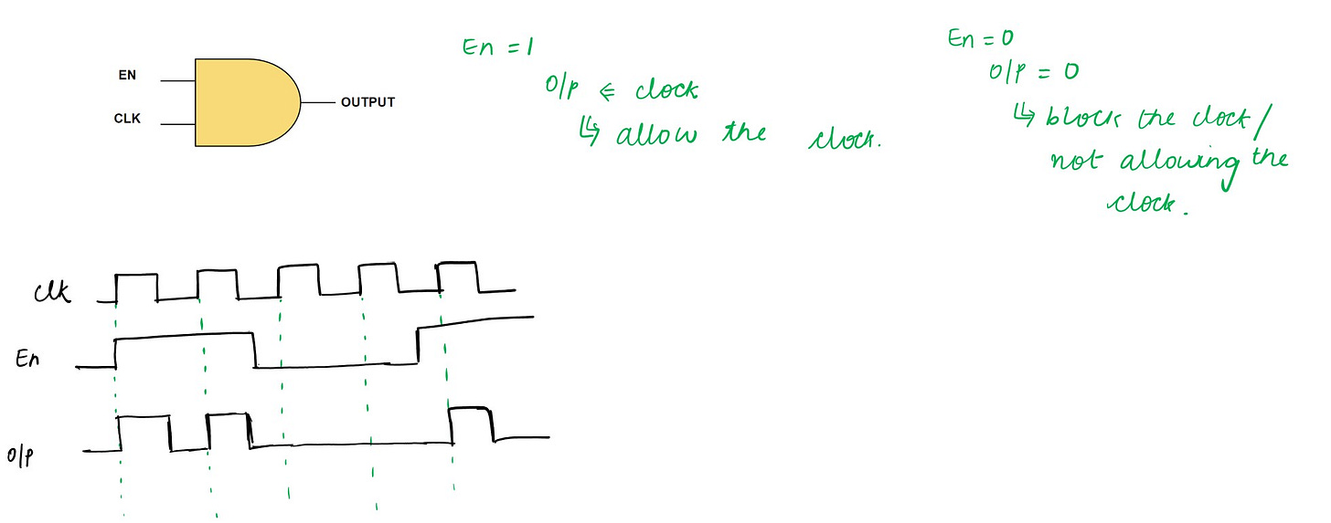
An And gate can be used as a clock gating cell.
For example,
In functional mode, only when we turn on the Bluetooth feature in our device, EN signal will be 1 (designed by the designer). Hence clock will be propagated to the Bluetooth module.
Otherwise, EN signal will be 0. Hence clock will not be propagated to the Bluetooth module.

• And gate used as clock gating cell has a disadvantage. It will produce glitches whenever enable is changing when clock is high .

We use Integrated Clock gating Cell (ICG) to avoid glitches.
Integrated Clock Gating Cell

This is an Integrated Clock Gating (ICG) cell.
FE is Functional Enable. It is specific to the functional team (which we have explored in the Bluetooth example).
TE is Test Enable. It is specific to DFT team.
A negative level triggered latch is used to avoid glitches.

Output of the ICG (last signal of the above waveform goes to the modules, example Bluetooth module)
How to control the TE (Test Enable) of ICG?
For functional team, all modules of a block are not operated at the same time (as we have explored above).
So functional team will stop the clock to the modules that are not operating at that time to minimize the dynamic power.
But for DFT team, the complete block will be stitched into scan chains. All the scan chains are operated parallelly.

So during DFT, we have to always propagate clock to the flops.
So we can connect the TE (Test Enable) of ICG to TM(Test Mode).
TM is used to distinguish between DFT mode and functional mode.
TM = 0, during functional mode (normal mode)
TM = 1, during DFT mode
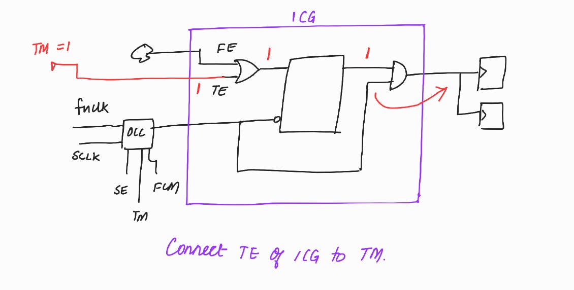
We can also connect the TE (Test Enable) of ICG to (SE) Scan Enable. This will be more advantageous.
< < We will explore about connecting TE of ICG to SE in detail during ATPG topic > >
