In this blog, we’ll take a deep dive into JTAG and IJTAG.
Here’s a quick overview of the key topics we’ll cover :
Need of JTAG
Minimizing the no. of top level ports using JTAG
JTAG Architecture
Test Access Port (TAP)
TAP architecture
TAP controller — Detailed View of Each State
Test_setup phase
Internal JTAG (IJTAG)
Two instrument network with SIBs
IJTAG network
SIB — Internal Architecture with Illustrations
SIB STI and SIB SRI
Block Level IJTAG — Detailed View of Each State
JOINT TEST ACTION GROUP (JTAG)
[IEEE 1149.1 std]
Need of JTAG :
• To minimize the no. of top level ports.
• To achieve boundary scan.
< < We will explore boundary scan in my DFT Basics Series. In this post, we will explore how we are able to minimize the no. of top level ports using JTAG. > >
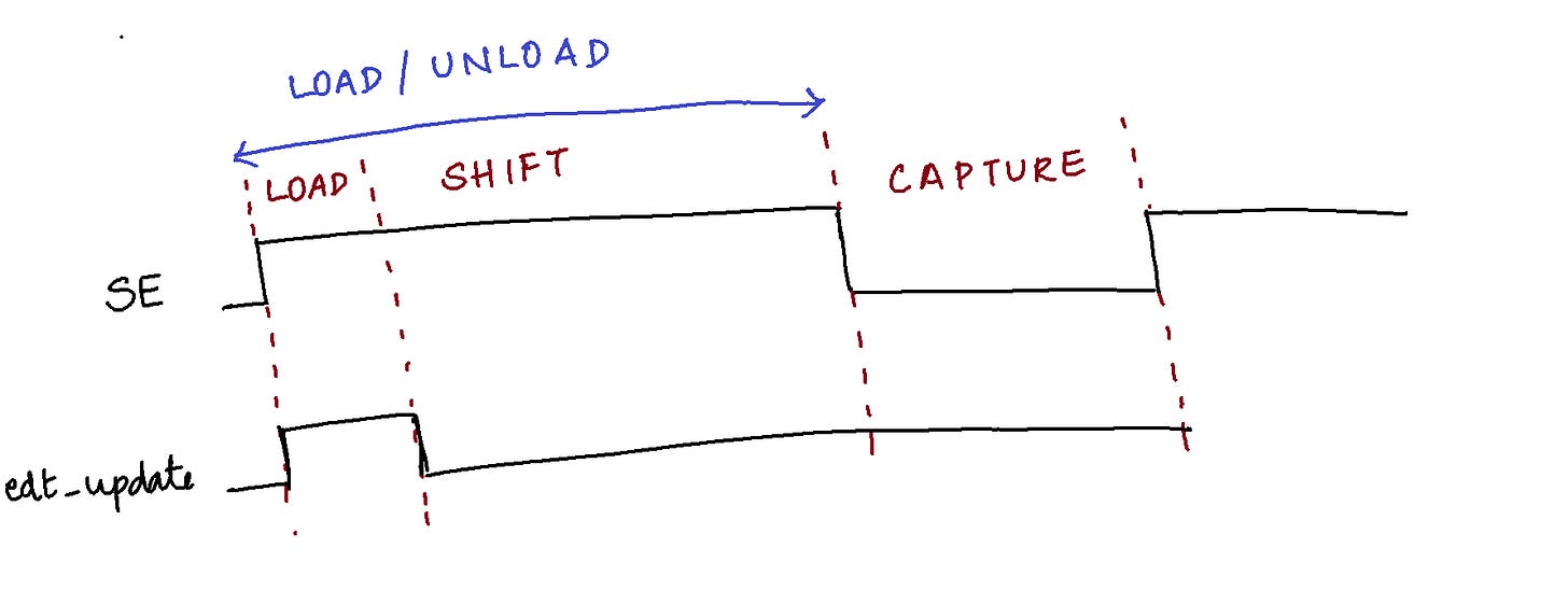
TM = 1 for the complete run. It can be controlled using JTAG.
edt_update => non static / dynamic signal
For the same run, during load it will be 1, for the rest of the procedures it will be 0. This can’t be controlled using JTAG. We have to control from top level.
SE => non static/ dynamic signal
SE = 1 => during load and shift
SE = 0 => during capture.
It can’t be controlled using JTAG. We have to control it from top level.
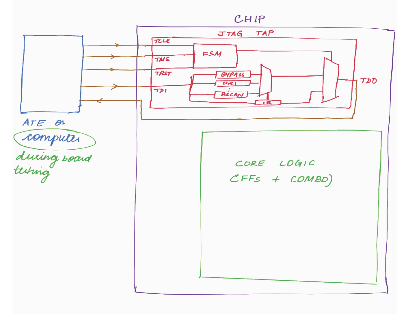
JTAG Architecture
JTAG consists of
• A TAP [Test Access Port]
• A TAP controller [16 state FSM]
• An instruction register [IR]
• A group of test data registers [TDRs]
Test Access Port (TAP)
It is the interface used for JTAG control.
The IEEE standard defines four mandatory TAP signals and one optional TRST signal.
1. TDI (Test Data Input)– Serial input for test instruction and data.
2. TDO (Test Data Output)– Serial output for test instruction and data.
3. TCK (Test Clock) – It is the clock to the Test Data Registers (TDR),
Instruction Register (IR).
4. TMS (Test Mode Select) – It controls the TAP controller’s state transitions.
5. [Optional] TRST (Test Reset) – Provides for asynchronous initialization of the TAP controller.
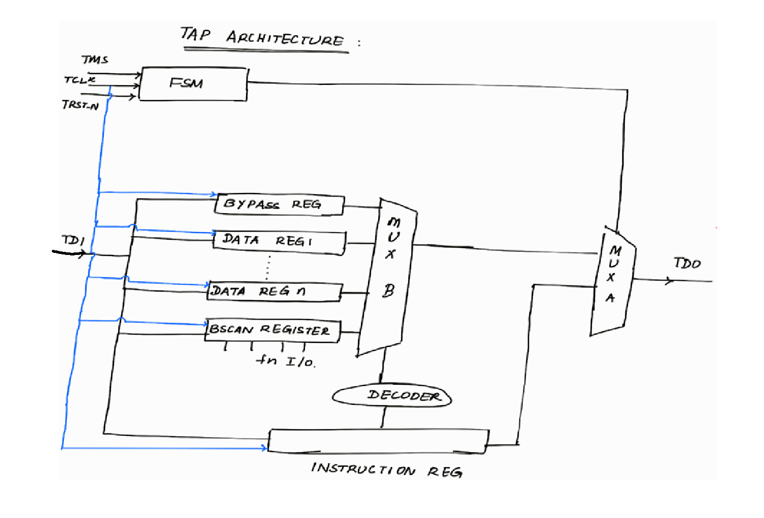
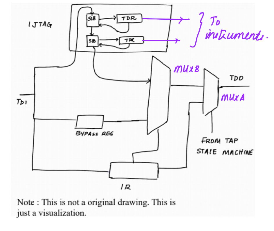
TAP Architecture
In the above figure,
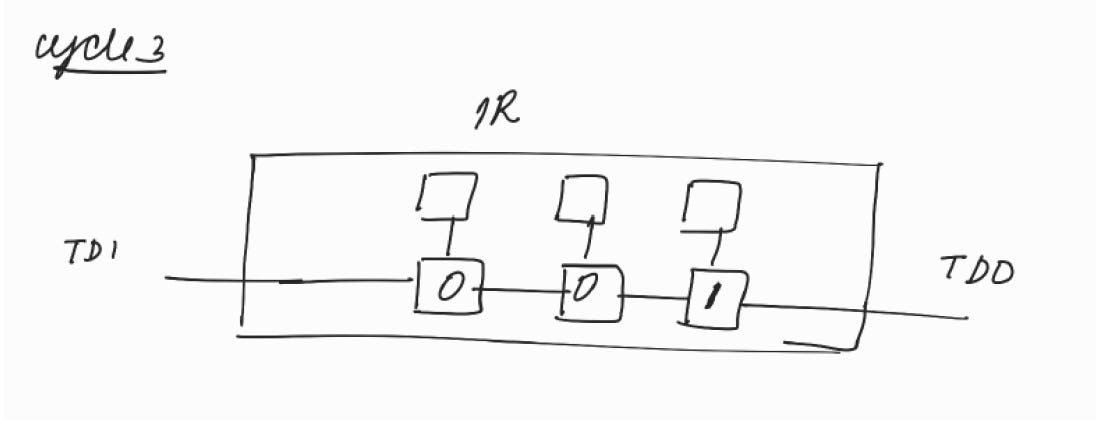
Mux A : It is to select between IR and DR. It’s selection line is from JTAG FSM (TAP controller). When FSM is in any one of the IR states, it will select IR else it will select DR.
Mux B : It selects one particular data register based on the instruction loaded into the instruction register. The output of instruction register will be given to a decoder. The output of decoder acts as the select line of mux B.
Need of Decoder : To reduce the no. of bits of the instruction register’s shift register and hold register.
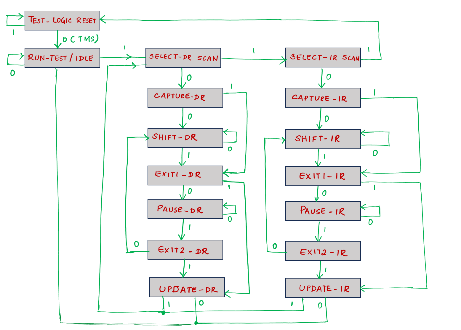
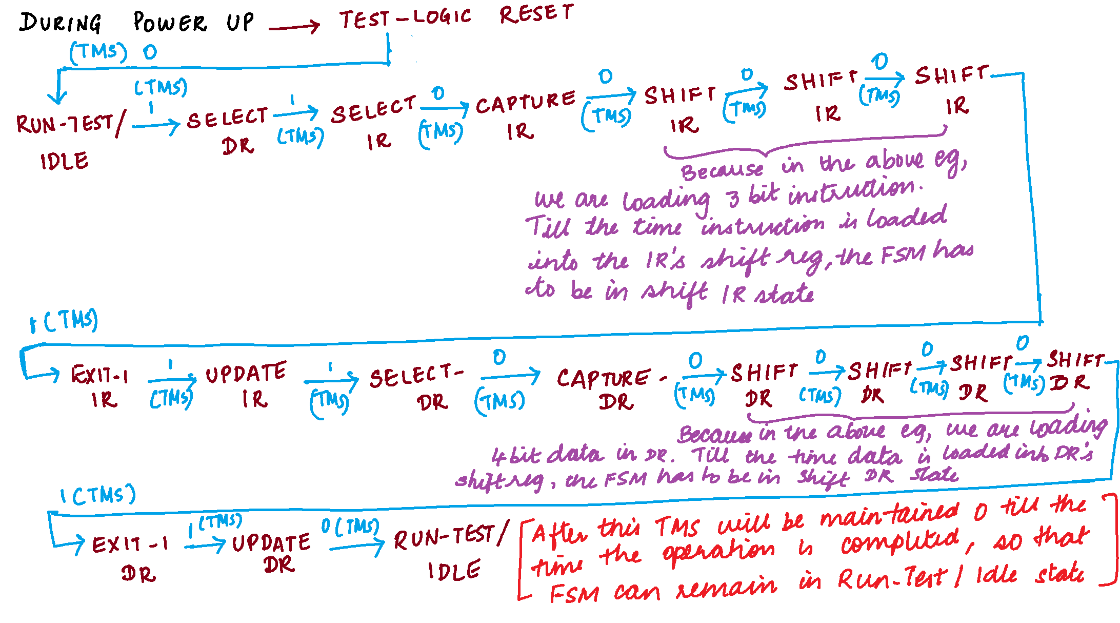
TAP Controller — Detailed View of Each State
It is a 16 state FSM.
Let’s explore the various states of JTAG FSM. We will also explore how we are able to internally control the static signals using JTAG.
Test-Logic-Reset state :
Test logic is disabled.
Normal operation of the chip can continue.
FSM enters this state
i. When TRST_N is pulled active (TRST_N = 0)
(or)
ii. When TMS input is held active for at least 5 clock cycles
iii. Upon power up (process of applying power to the entire chip
[including the JTAG module]. When power is applied, JTAG FSM enters the
rest state)
Run-Test/Idle:
This is a state in which the FSM is waiting for some test operations to complete.
Example :
If we are going to do core-logic test for a block, then the following signals
(int_mode, ext_mode, int_ltest_en, ext_ltest_en )will be controlled to their
appropriate value through TDR to start the operations.
Till the time core-logic test completes, the FSM will be in the Run-Test/Idle
state.
Select-DR/Scan and Select-IR/Scan :
Temporary state to initiate the test data sequence for IR/DR respectively.
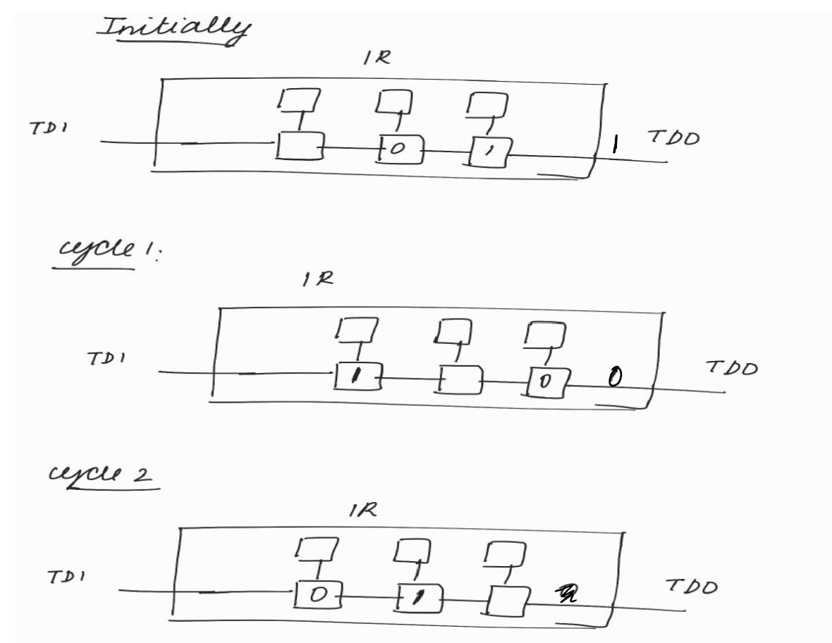
Capture-IR :
The shift register contained in the instruction register loads a fixed value
(two LSB are 0 and 1).
This is done to check whether there is any SA0 and SA1 fault in the TDI and
TDO line.
Shift-IR :
During this state, the required instruction will be serially loaded into the shift
register inside the instruction register.
For each clock cycle (TCK), one bit is shifted in and out of instruction register
through TDI and TDO.
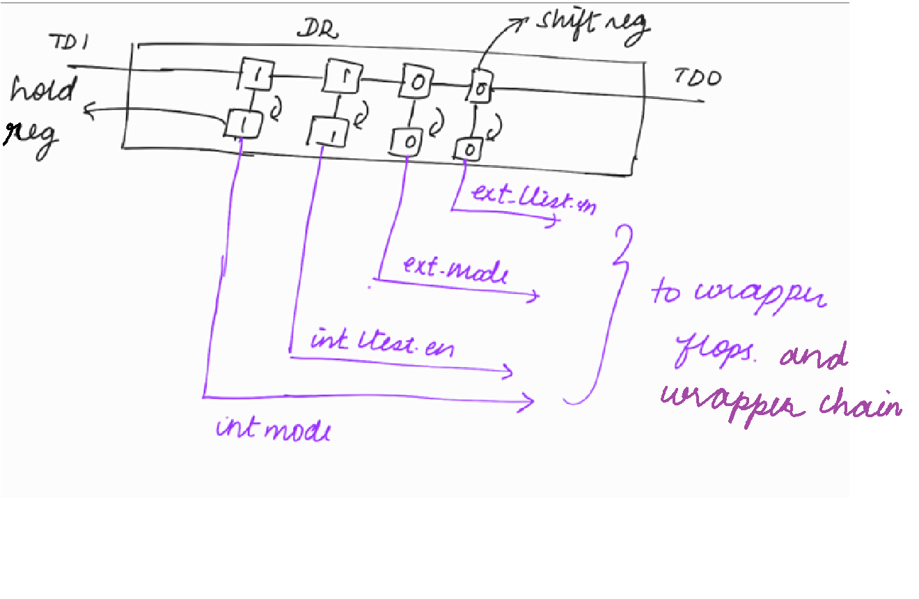
Illustration :
Suppose if Data reg 1 is to be selected and the instruction to select DR1 is 001,
then the required instruction will be loaded into the IR’s shift register during
shift IR state.
Note :
Explanation of no. of bits in the IR :
There are 3 mandatory JTAG instructions : Extest, Sample Preload, Bypass < < We will explore these instructions in Boundary Scan topic in my DFT Basics
Series > >
IR must be at least 2 bit wide in order to select these mandatory instructions.
The size of IR can be increased based on the no. of TDRs we are having.
Exit1- IR :
It is a temporary state
If TMS is held high, the controller enters the update-IR state which terminates
the scanning process.
Pause-IR :
Allows shifting of IR to be temporarily halted.
< < We will explore the significance of this state in the later part of the blog (Significance of Pause State section) > >
Exit2- IR :
A temporary state
TMS is held high, the controller enters the update-IR state which terminates
the scanning process.
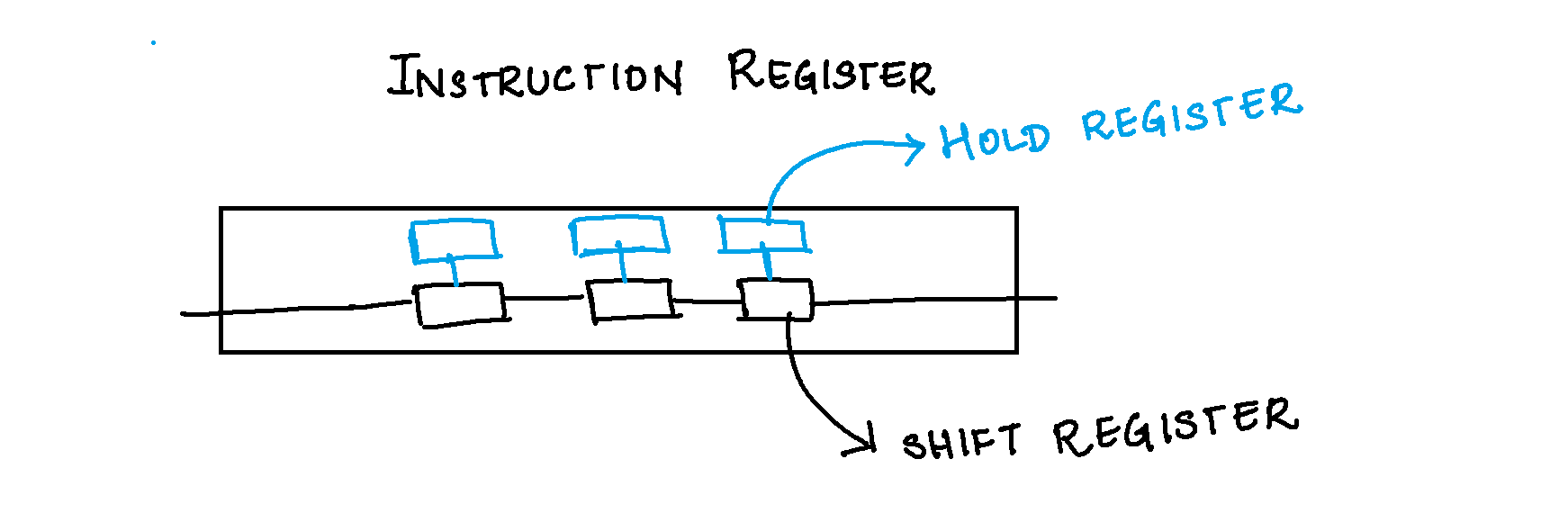
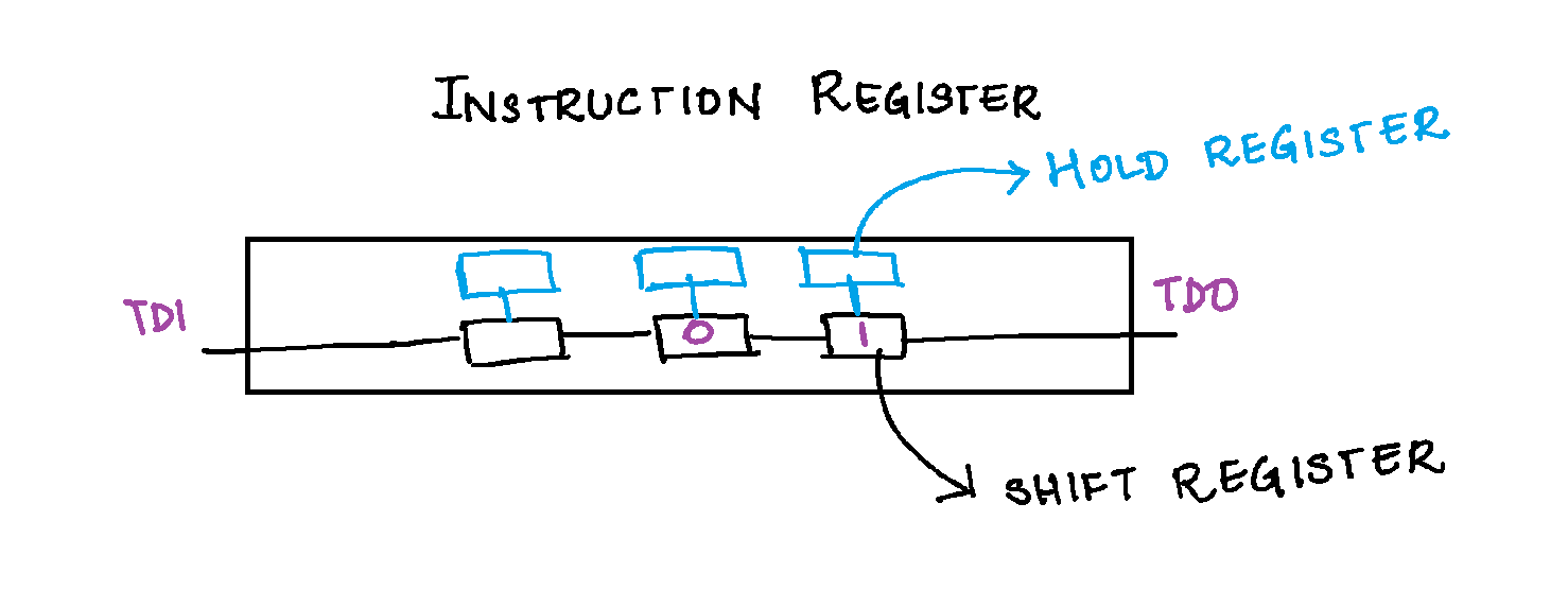
Update-IR :
The instruction which has been shifted into the IR’s shift register is parallelly loaded into the IR’s hold register.
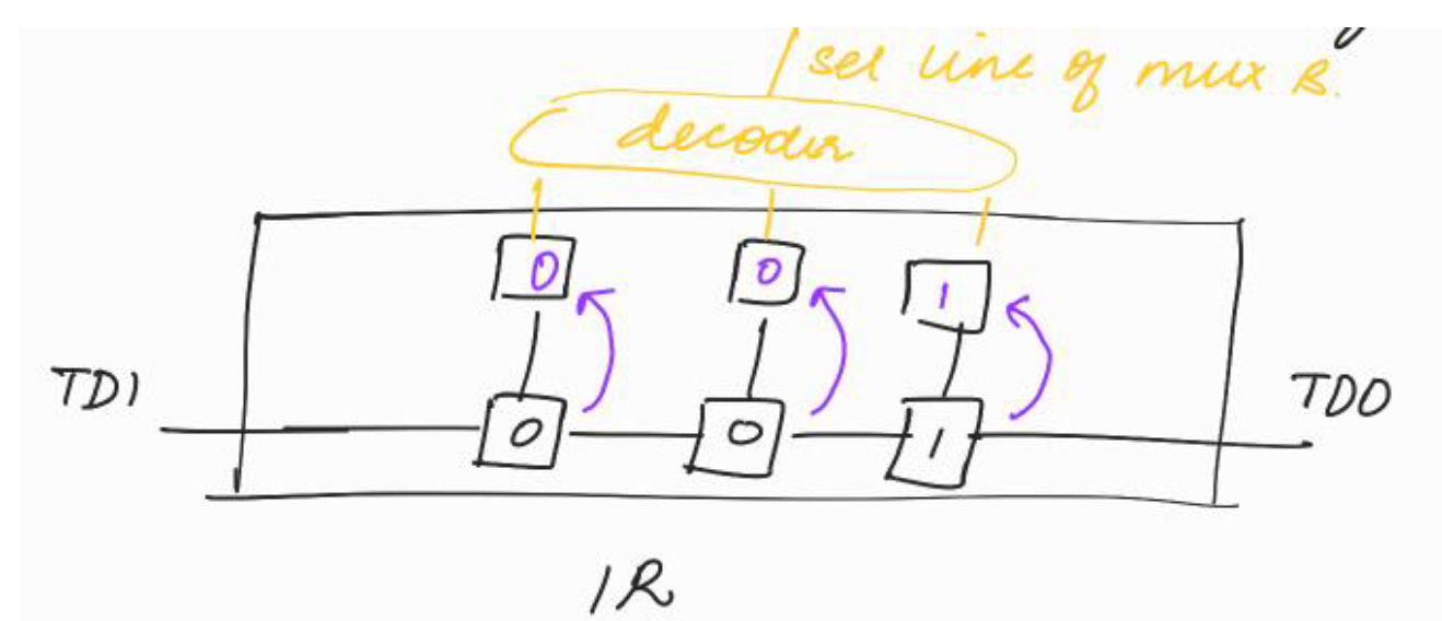
Capture-DR :
Data may be parallelly loaded into the test data register that is selected by the current instruction.
Shift-DR :
During this state, the required data will be serially loaded into the shift register
inside the Data register.
For each clock cycle (TCK), one bit is shifted in and out of data register through
TDI and TDO.
Illustration
If DR1 is used for core test control. It controls these signals: int_mode, ext_mode, int_ltest_en, ext_ltest_en < < We will explore all these signals in the Hierarchical Scan topic in DFT Basics Series > >
Suppose we are doing the core-logic test of a block: int_mode = 1, ext_mode = 0, int_ltest_en = 1, ext_ltest_en = 0
After 4 cycles of TCK
Exit1- DR :
It is a temporary state.
If TMS is held high, the controller enters the update-DR state which terminates
the scanning process.
Pause-DR :
Allows shifting of DR to be temporarily halted.
< < We will explore the significance of this state in the later part of the blog (Significance of Pause State section) > >
Exit2- DR :
It is a temporary state.
If TMS is held high, the controller enters the update-DR state which terminates
the scanning process.
Update-DR :
The data which has been shifted into the DR’s shift register is parallelly loaded into the DR’s hold register.
< < We will explore all these signals and wrappers during Hierarchical Scan Topic in DFT Basics Series > >
The illustration above demonstrates how static signals can be controlled using JTAG
Significance of Pause State :
For loading some patterns, say for example, ATE is small and is not having memory to load the complete pattern, in that case, the patterns will be divided into two.
After loading the first half FSM will be in pause state, then after refreshing the ATE memory, shifting will continue to load the second half
Let’s summarize
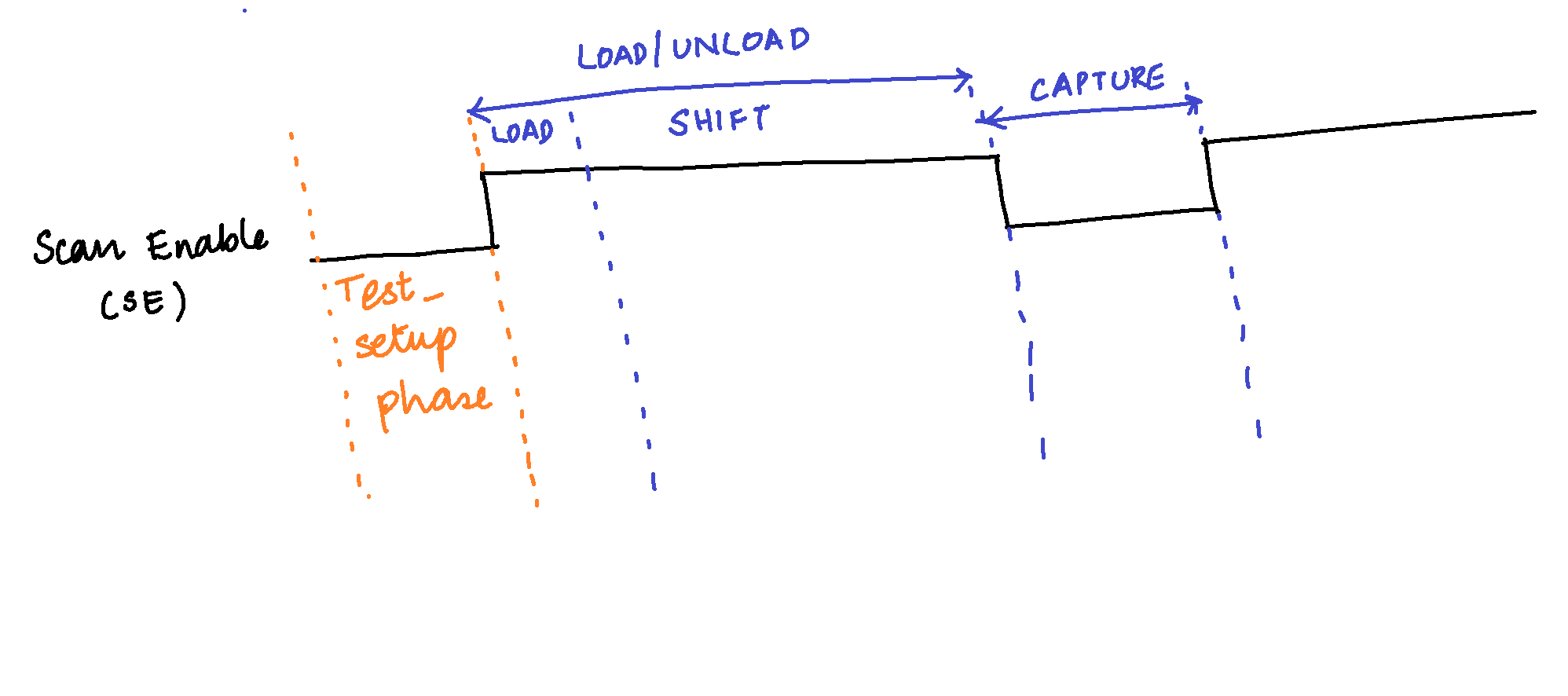
Test_Setup Phase
The TDRs will be loaded in the test_setup phase.
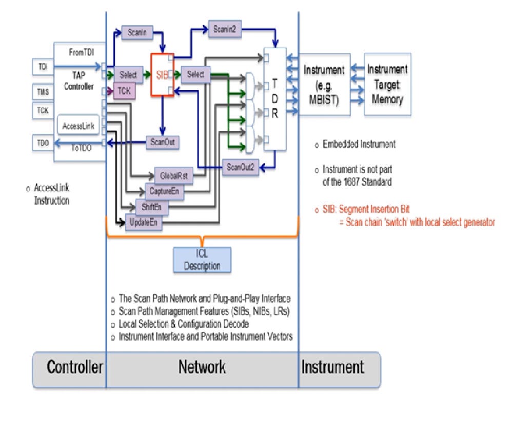
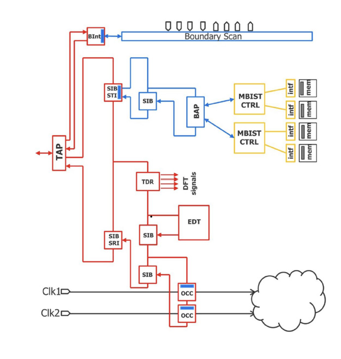
INTERNAL JTAG (IJTAG)
IEEE 1687 Std
Image Source : Tessent Documentation
Controller : TAP + FSM
Network : SIB + TDR
Instrument : What is being controlled
For example, MBIST controller
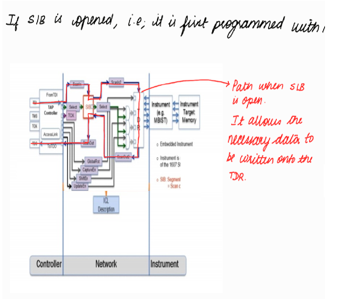
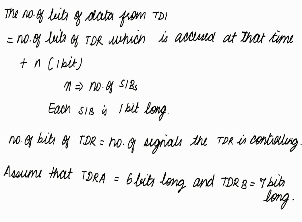
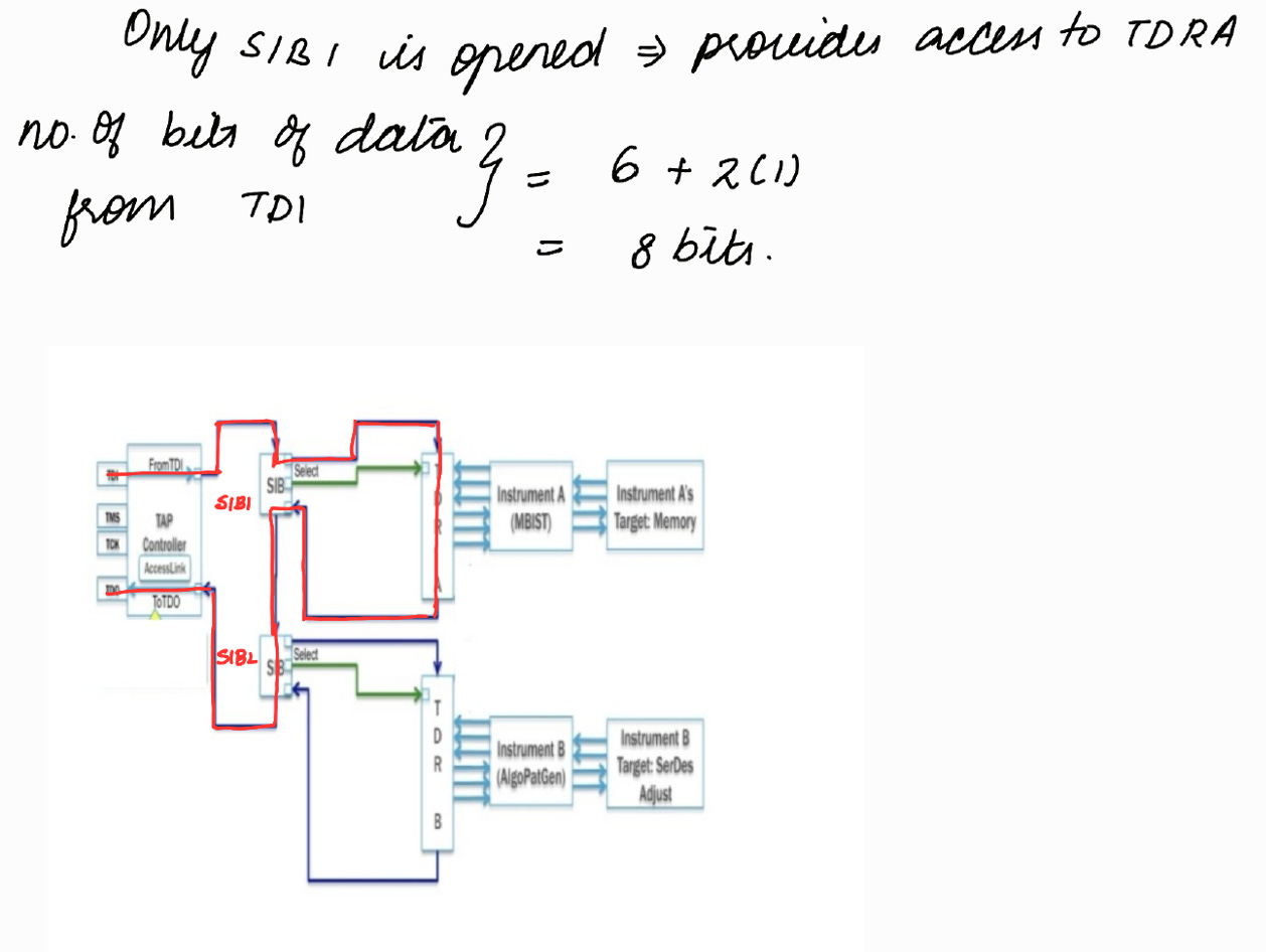
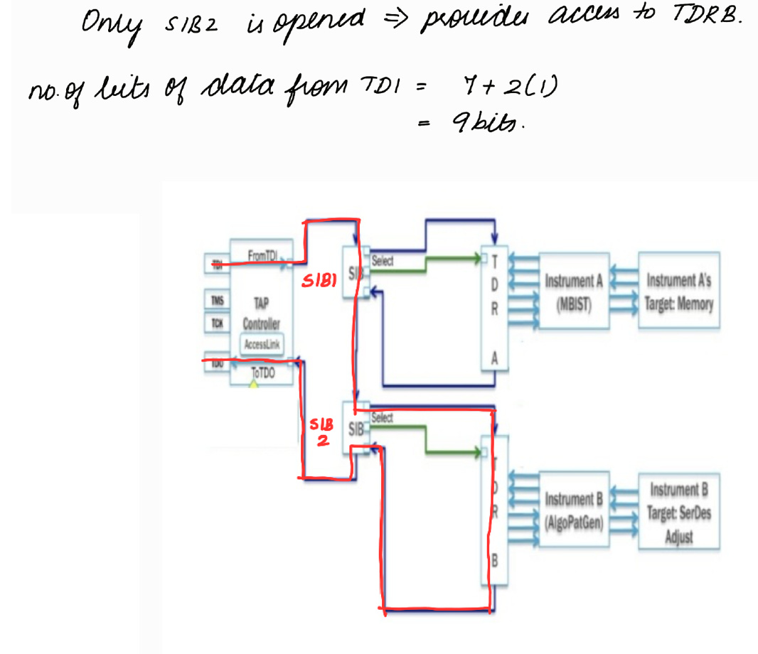
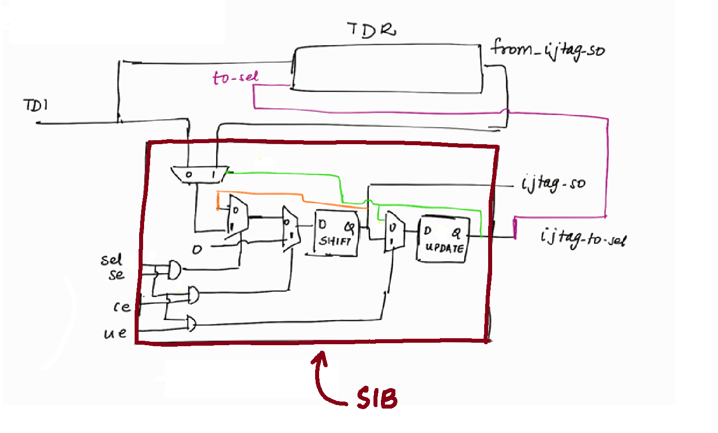
In IEEE 1687 std (IJTAG), there is an additional component - Segment Insertion Bit (SIB)
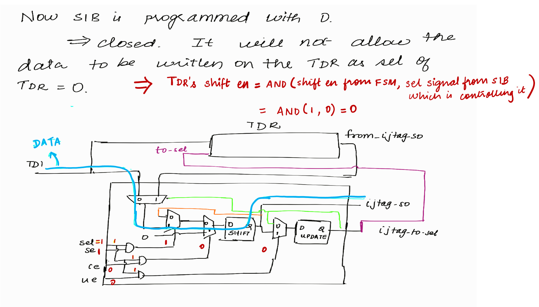
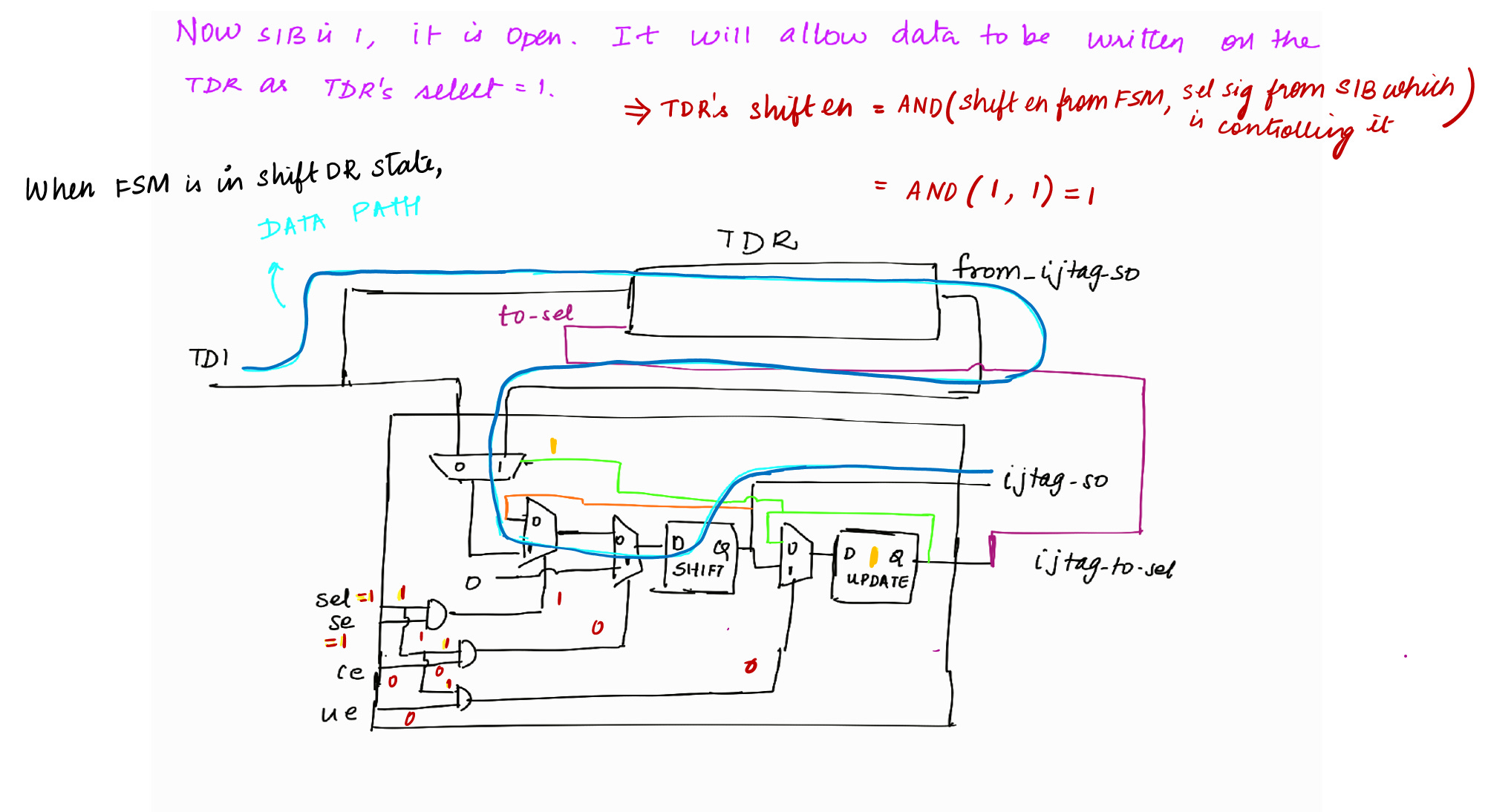
When SIB is programmed with 1, it means that the SIB is open. If SIB is opened, it provides access to the TDR (It allows the necessary data to be written onto the TDR)
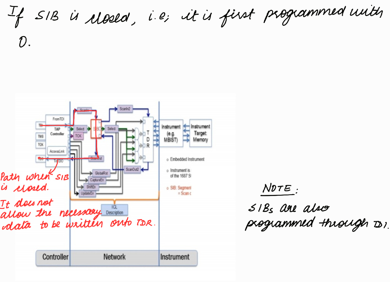
When SIB is programmed with 0, it means that the SIB is closed. If SIB is closed, it does not provide access to the TDR.
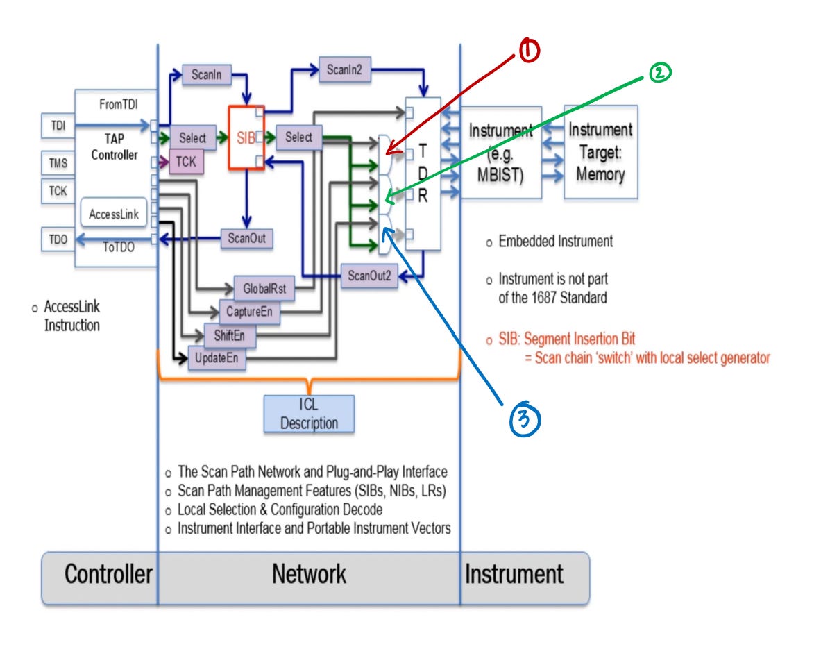
Control Signals :
Global Reset
Capture En
Shift En
Update En
FSM is in capture DR sate, Capture En = 1
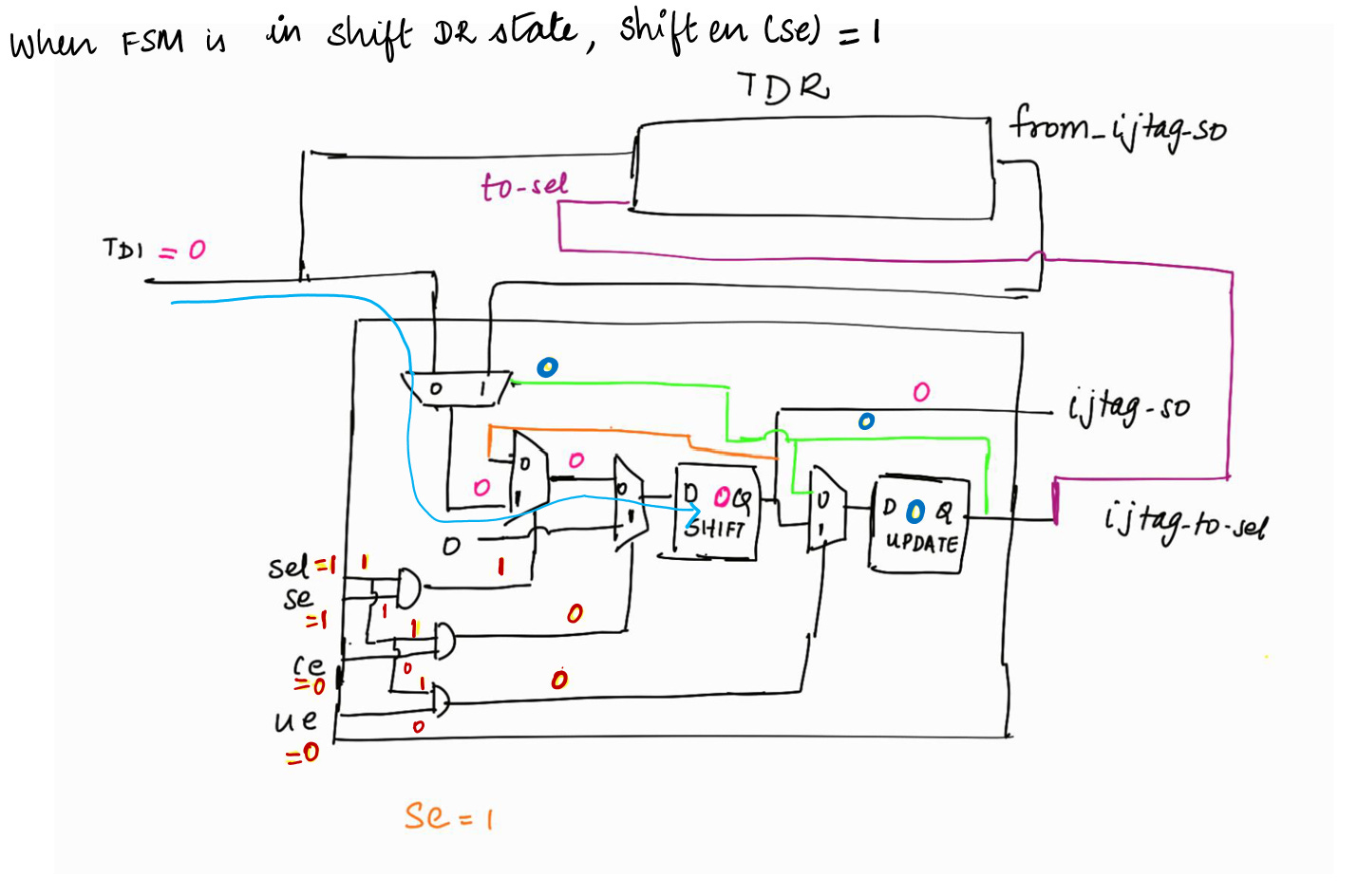
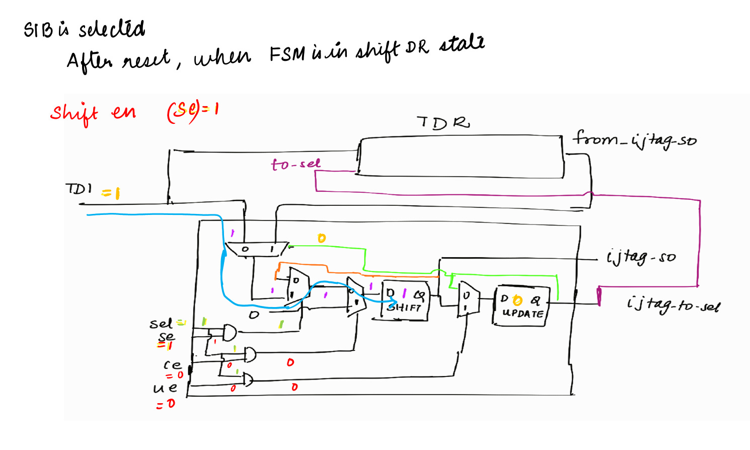
FSM is in shift DR sate, Shift En = 1
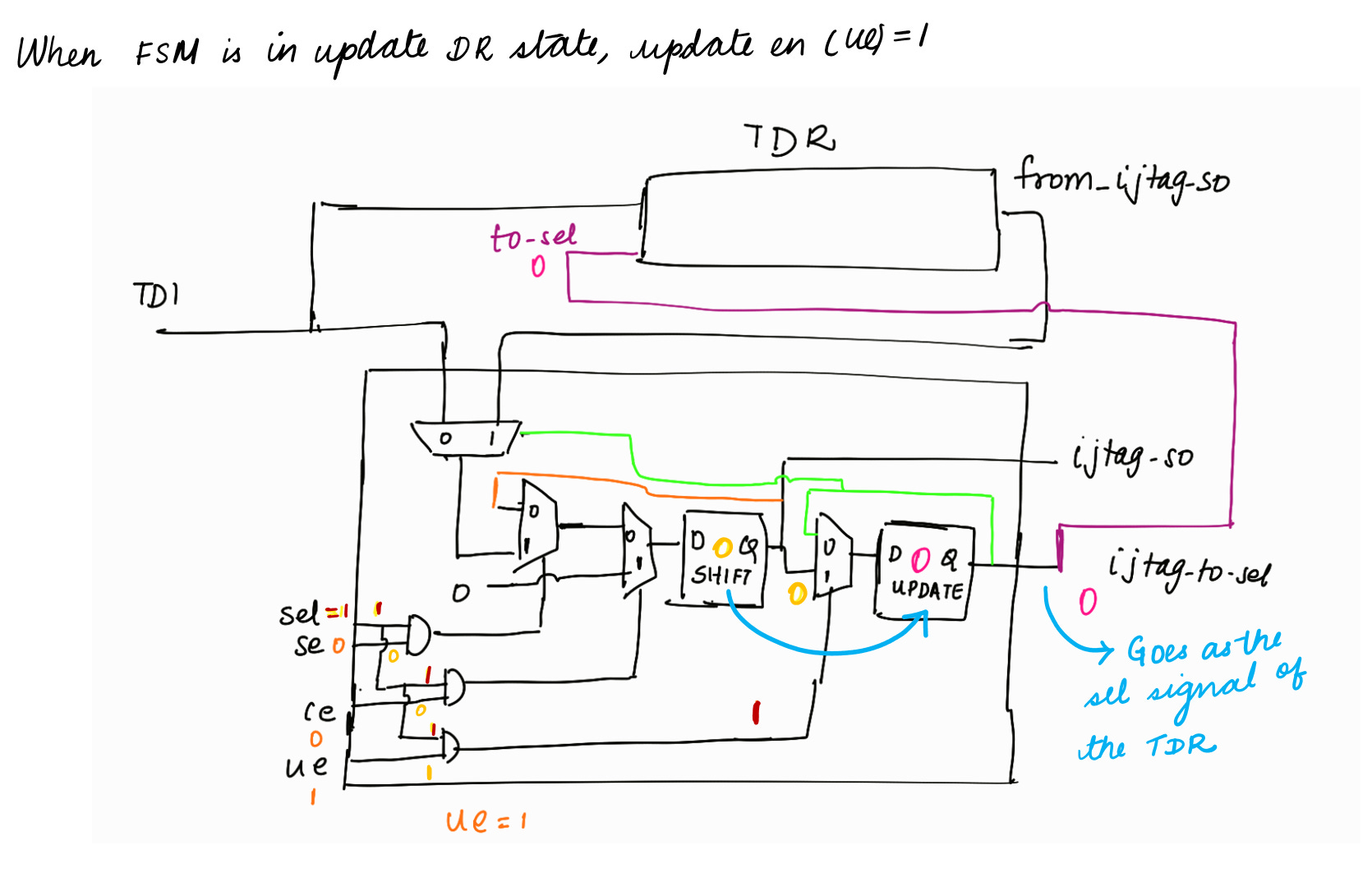
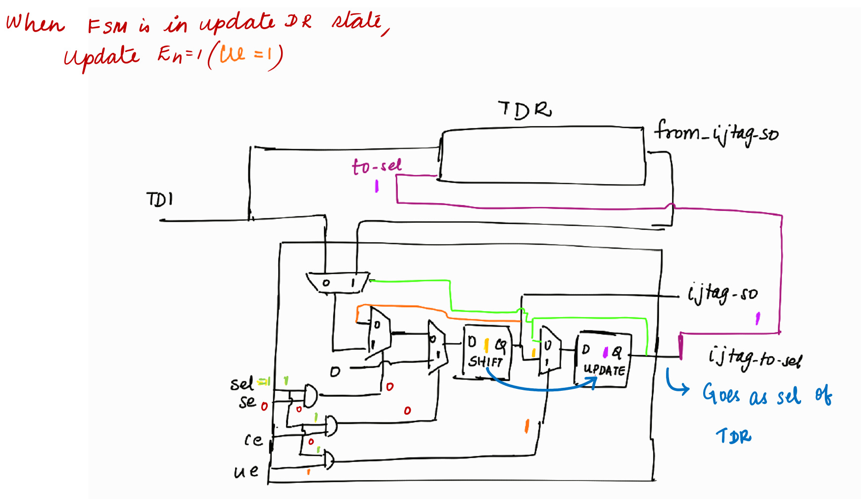
FSM is in update DR sate, Update En = 1
Whenever Global Reset is pulsed, it reset the DRs and IR
TDR’s capture En = and (capture En from FSM, select signal from SIB) [marked as 1 in the below figure]
TDR’s shift En = and (shift En from FSM, select signal from SIB) [marked as 2 in the below figure]
TDR’s update En = and (update En from FSM, select signal from SIB) [marked as 3 in the below figure]
When SIB is programmed with 1, select = 1
When select = 1 and shift En from FSM = 1 => shifting of required data will happen on TDR
When select = 1 and Update En from FSM = 1 => value which is present in the shift register of TDR will be loaded on to the hold register present inside TDR
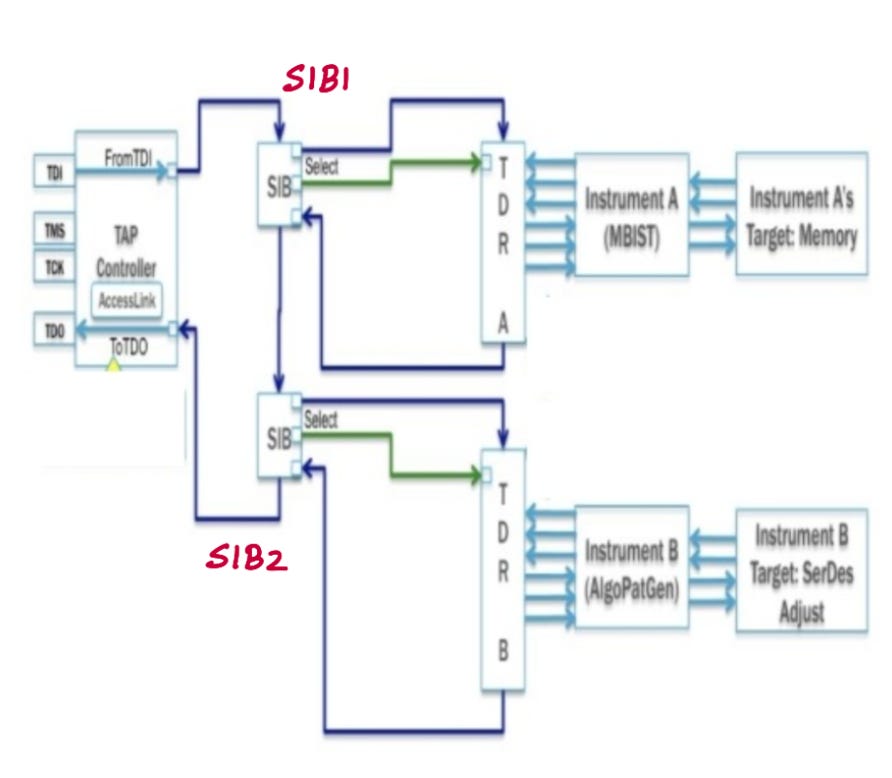
A Two Instrument Network with SIBs
Image Source : IEEE 1687 IJTAG | THE FUTURE OF EMBEDDED INSTRUMENTS
IJTAG network
A single IR-scan is required to access the IJTAG network, then DR-scans can open one or the other, or both of the instruments’ SIBs.
Explanation of the above point : • When IR is selected, the required instruction is shifted into the shift register present in IR through TDI.
• In the Update IR state, the instruction which has been shifted into the IR’s shift register will be loaded onto the hold register present inside IR.
• The output of IR is given to the decoder which goes as a select line to mux B.
• If IJTAG is selected, then during DR scan (i.e., during Shift DR state), the SIBs and TDRs are programmed with their appropriate values.
• In Update DR state, data from the shift register in the SIB and in the selected TDR is loaded into the hold register. The output of the selected TDR is given to the instruments.
SIB — Internal Architecture with Illustration
Note : The figure above provides a high-level view of the internal structure of the SIB. It is intended to illustrate the main components and their interactions, but it should not be interpreted as the precise architectural layout.
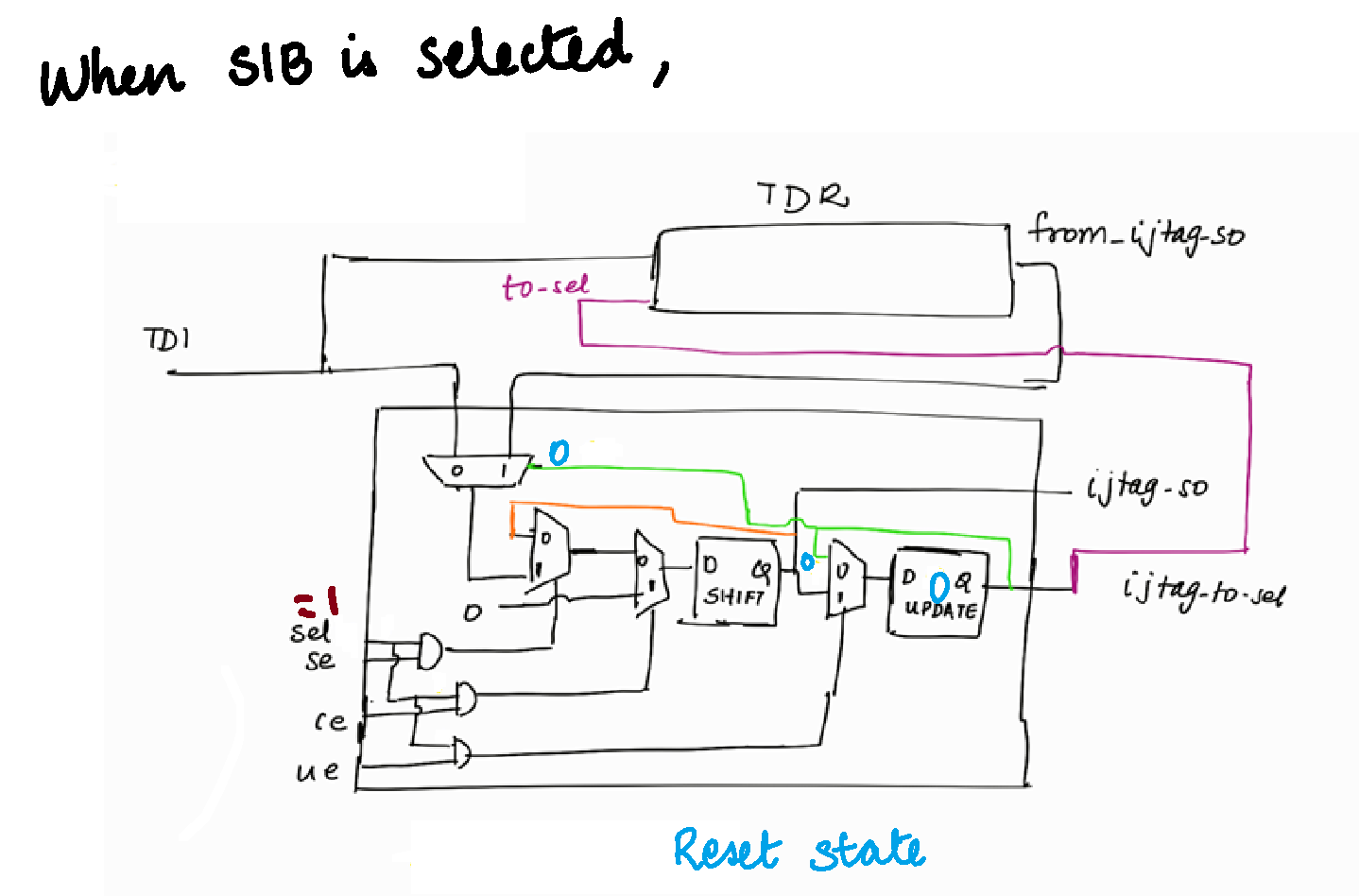
Figure 1 to Figure 4 illustrates SIB is closed case
Figure 1 : After Reset
Figure 2 : When FSM is in shit DR state
Figure 3 : When FSM is in Update DR state
Figure 4 : Path when SIB is closed
Figure 5 to Figure 7 depicts SIB is open case
Figure 5 : When FSM is in Shift DR state
Figure 6 : When FSM is in Update DR state
Figure 7 : Path when SIB is open
Note : If SIB is not selected, the last updated value of the SIB has to act as to_select of TDRs or other SIBs till it is reset.
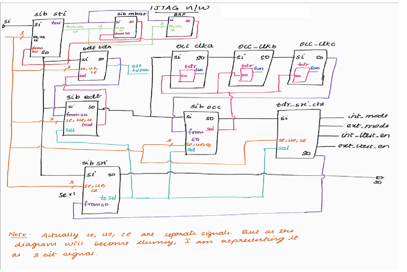
SIB STI and SIB SRI
Image Source :Example IJTAG network implementation - End-to-end automation is the next leap forward for DFT
A SIB is a special node in IJTAG that acts as a switch.
Instruments that need to be active during scan (EDT OCC) are inserted under 1 SIB and the ones that are scan tested such as MBIST controller are inserted under another SIB.
Scan Tested Instrument (SIB STI) : SIB STI provides access to the IJTAG network for the instruments that are scan tested. SIB STI provides access to the IJTAG network for MBIST controller (in the above figure)
Scan Resource Instrument (SIB SRI) : SIB SRI provides access to the IJTAG network for the instruments that need to be active during scan.
SIB SRI provides access to the IJTAG network for logic instruments (EDT OCC)
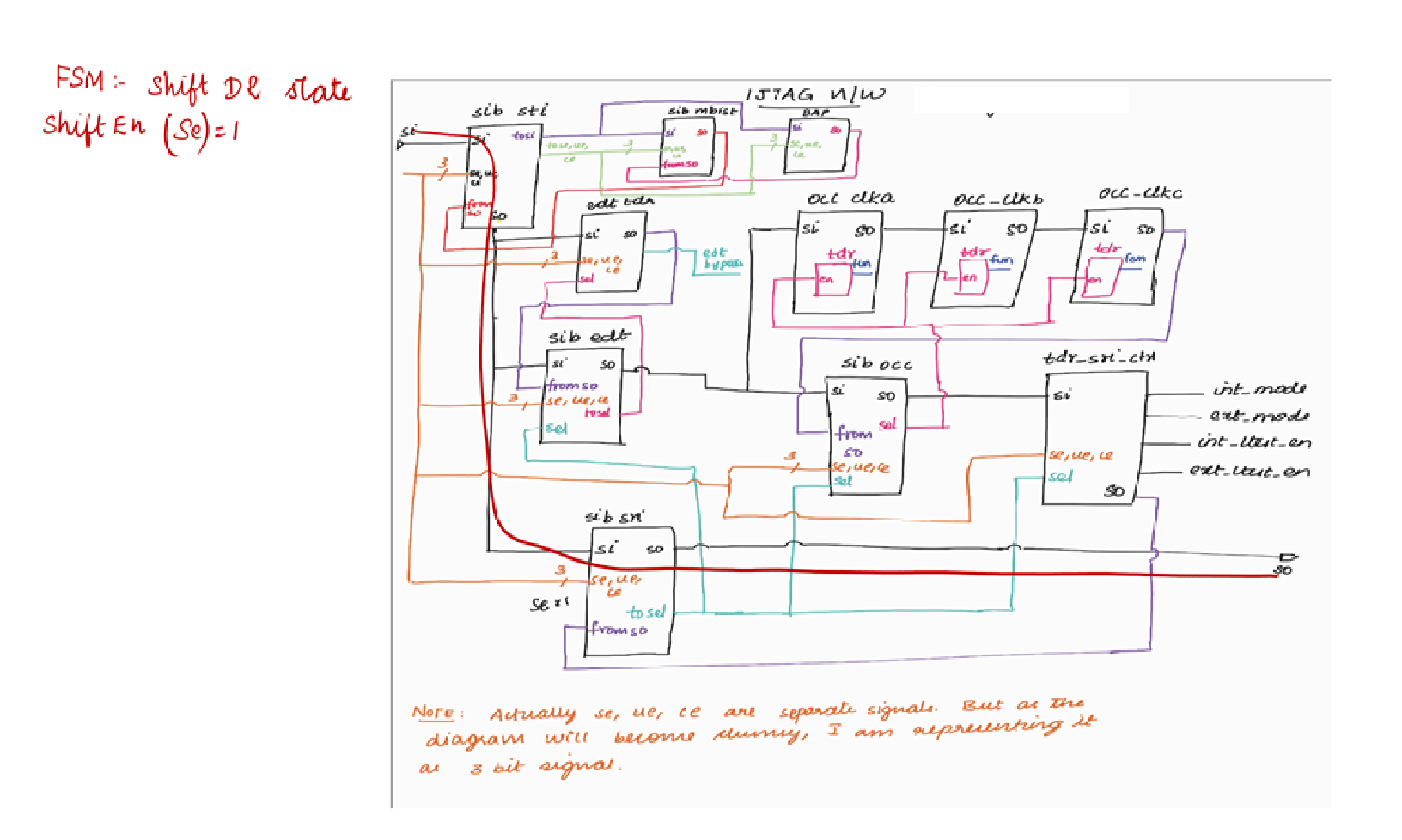
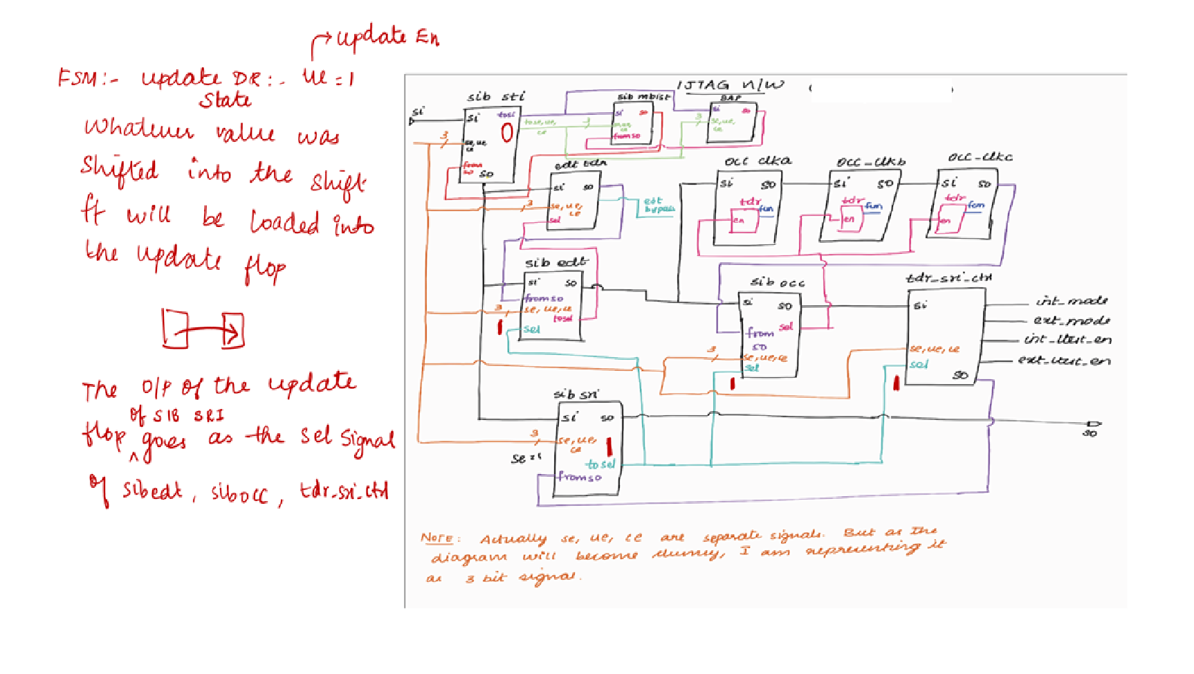
Block Level IJTAG — Detailed View of Each State
The above figure illustrates the IJTAG network within a block.
Note : An understanding of the IJTAG network within a block builds upon the internal structure of the SIB, introduced in the previous section.
Suppose, we are going to do the core logic test of a block :
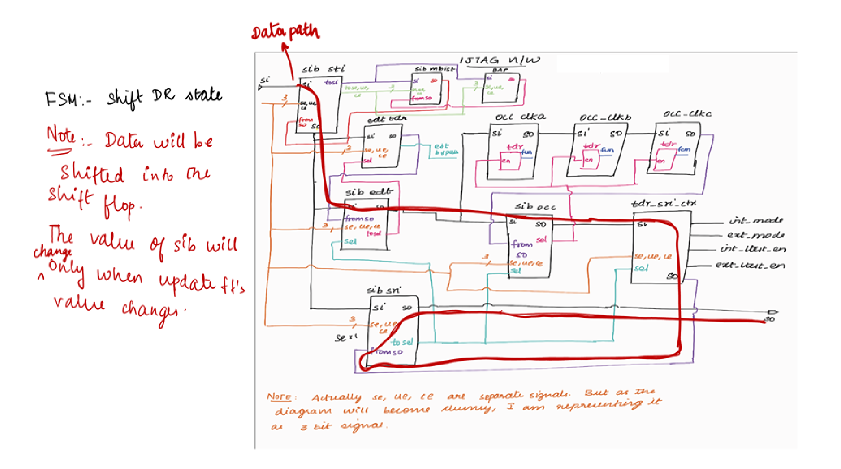
Figure 1 : When FSM is in Shift DR state
When FSM is in Shift DR state, shift_en = 1.
Shifting of required data will happen in sib_sti and sib_sri (as shown in the above figure).
The shift register present inside sib_sri will be loaded with 1.
Figure 2 : When FSM is in Update DR state
When FSM is in update DR state, Update En = 1. The value which is present inside sib_sti’s and sib_sri’s shift flop will be loaded into the hold flop (or) update flop present inside them (as shown in the above figure).
Now sib_sri is programmed with 1.
As a result, the select signal of sib_edt, sib_occ and tdr_sri_ctrl is 1.
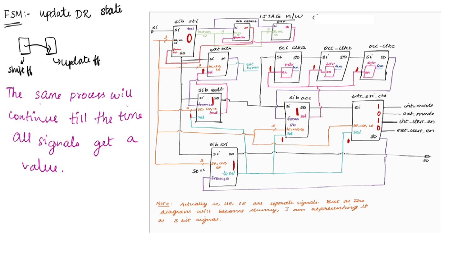
Figure 3 : When FSM is in Shift DR state
When FSM is in shift DR state Shift En = 1, and as the select signal of sib_edt, sib_occ and tdr_sri_ctrl is 1, the required data will be shifted into them (as shown in the above figure)
Figure 4 : When FSM is in Update DR state
When FSM is in Update DR state Update En = 1, and as the select signal of sib_edt, sib_occ and tdr_sri_ctrl is 1, the value which was loaded in the shift register present inside them will be loaded into the hold register present inside them (as shown in the above figure)
The same process will continue till the time all the signals get a value.
In this blog, we explored the fundamentals of JTAG and IJTAG networks and understood their importance.
In Part 2, we will focus on a detailed comparison between JTAG and IJTAG, highlighting the key advantages of IJTAG.
In Part 3, we will move towards application-oriented learning by discussing common interview questions related to JTAG.


Thank you.
Sure. I will finish the JTAG series and then write a post on hierarchical scan. I will explain scan wrappers in that post.
I will also post a series on MBIST and Tessent MBIST in future.
Waiting for your MBIST and SSN explanation