In my DFT Basics series, I’ve previously discussed various concepts around scan compression — including a detailed exploration of the EDT architecture, which is the scan compression strategy used by Mentor Graphics.
Recently, I’ve started learning about the CODEC-based scan compression architecture used in Synopsys tools. In this post, I’d like to share some of my initial learnings and observations about the CODEC — how it works and how it differs from EDT.
Note for Readers: To make the most out of this post, I recommend having a prior understanding of Scan Insertion, Scan Compression, and the basics of Fault Simulation. These foundational topics are already covered in my DFT Basics blog series, and they will help in better grasping the concepts discussed here.
I am still in the learning phase when it comes to Synopsys architectures. This post is based on my current understanding, so I encourage readers to treat this as a learning note, not an authoritative reference.
Corrections and insights are always welcome!
Let’s get started !
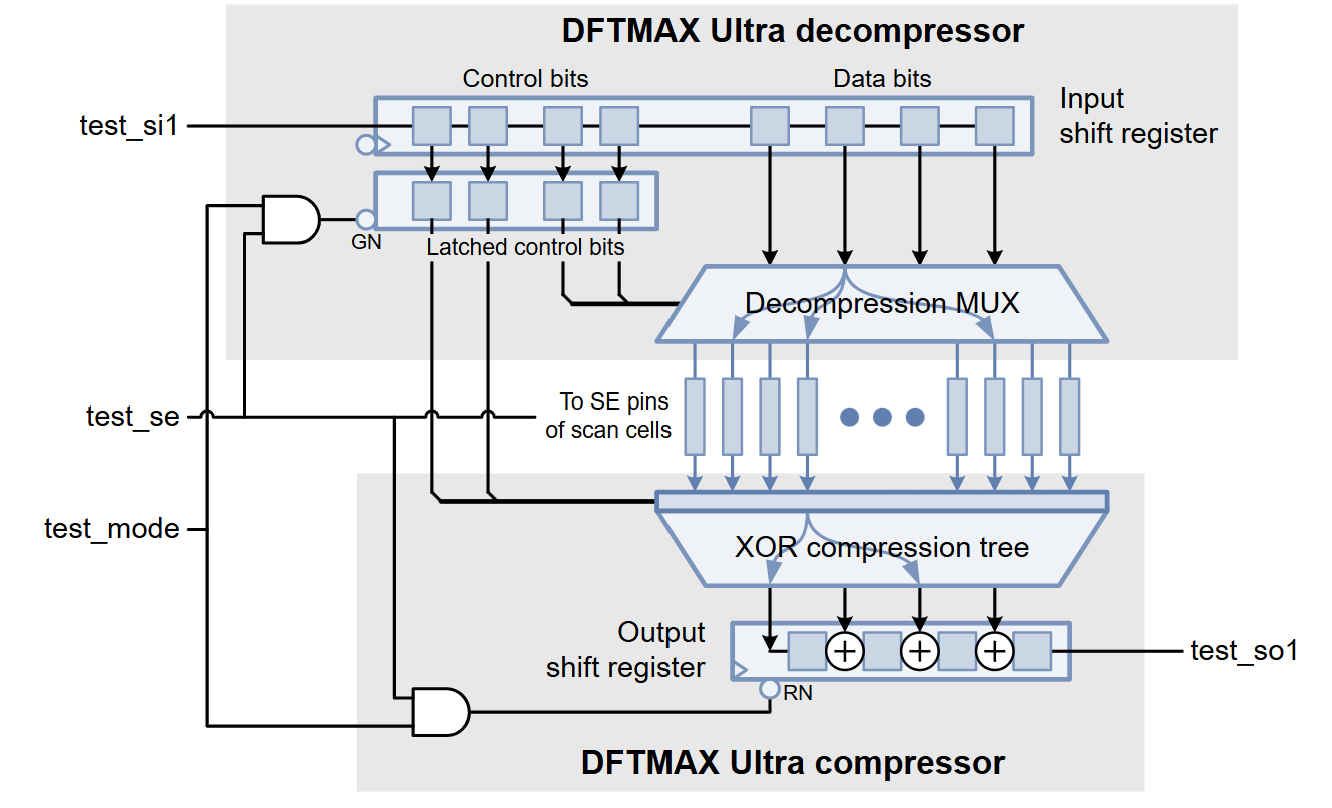
DFTMAX Ultra Compression Architecture
Figure 1 : DFTMAX Ultra Compression Architecture
Image Source : Solvnet - (Synopsys Documentation)
Input Shift Register and Decompression MUX
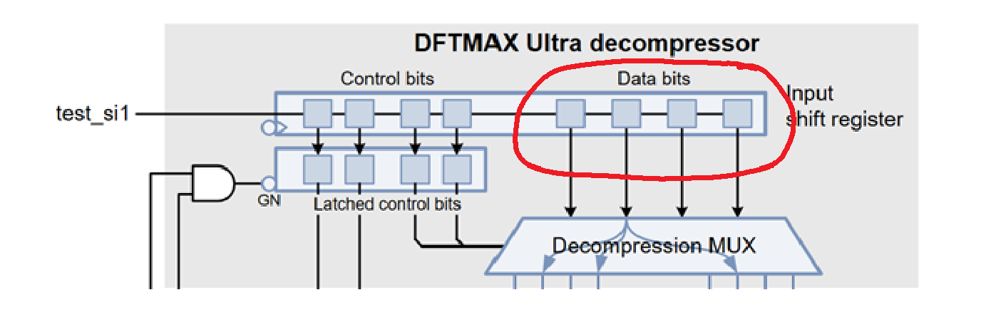
The input decompressor circuit uses a shift register and a decompression multiplexer (MUX). The input scan data at the scan-in pin feeds into the shift register, which is clocked on the trailing clock edge at the normal scan clock rate.
In this implementation example, the register has eight bits. The four register bits farthest from the scan-in pin feed into the decompression MUX (encircled register bits in the below figure).
Figure 2 : Input Shift Register and Decompression Mux
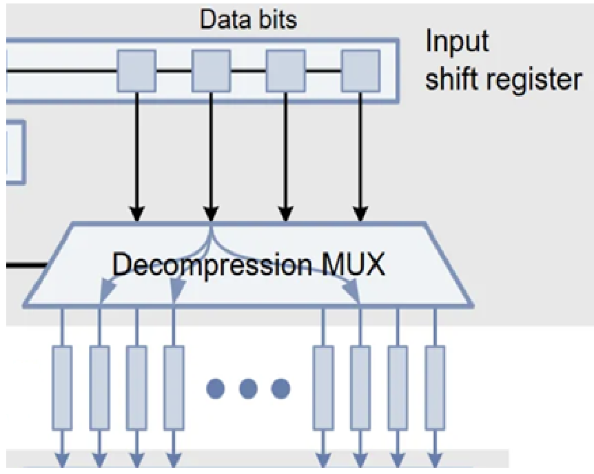
The decompression MUX is a combinational logic block that causes each of the four scan data bits to fan out to multiple scan chains.
The mapping of the four bits from the shift register to the scan chains remains constant for a particular pattern. However, the mapping can change from one pattern to the next.
Figure 3 : Input Shift Register and Decompression Mux
The mapping is controlled by bits in the control register (which will be explored in the later part of the blog). The shift-register structure that feeds into the decompression MUX causes the input data to stream into the scan chains multiple times.
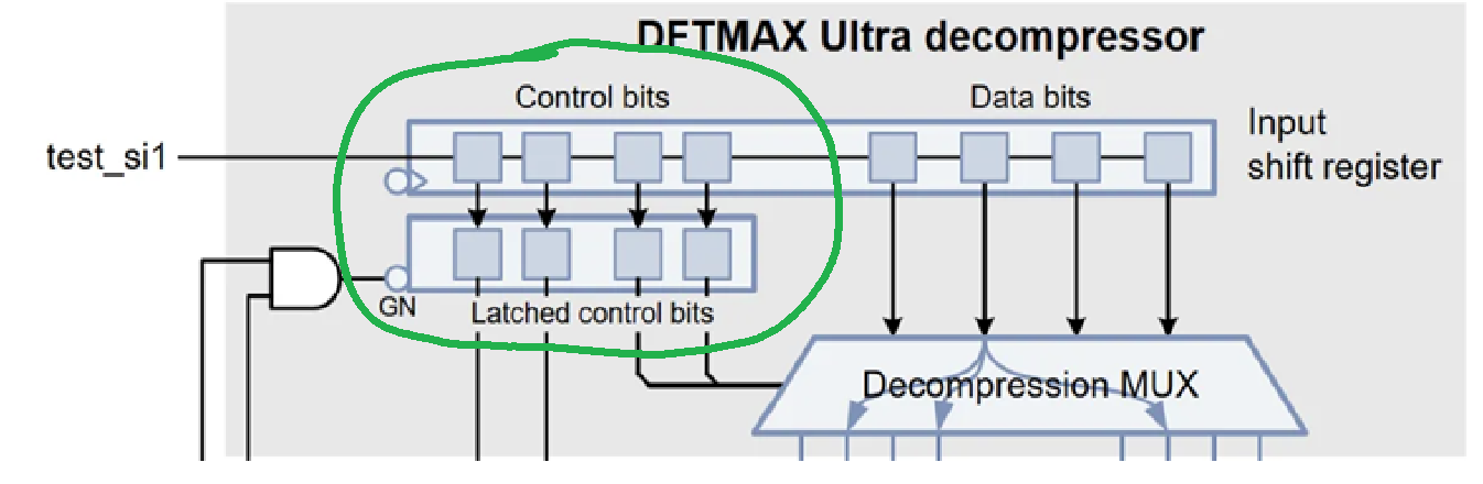
The encircled bits (in Figure 4) in the shift register are latched into the control register when the scan enable signal, test_se, is de-asserted. This de-assertion occurs exactly once per pattern.
Figure 4 : Control Register
Decompression Mux
The role of decompressor is to decompress the data at it’s input and apply a unique sequence into each of the internal scan chains. < < The combo logic between 2 flops will be different. We need to load an input sequence into the internal scan chains to test the respective combos. So we need to load an unique sequence into each of the internal scan chains > >
The load decompressor is designed to minimize dependencies (i.e., chains loading the same data in any mode).
Chains loading the same data in any mode could result in increased pattern count and loss of test coverage.
So load decompressor is designed to minimize dependencies.
Let’s explore how the decompression Mux structure is decided using the below example. < < Note : This example is not related to Figure 1 in terms of configurations. This example is just to illustrate how the decompressor mux structure is decided for a given configuration. > >
Figure 5 : Decompression Mux Architecture
Image Source : Minimizing the impact of Scan Compression
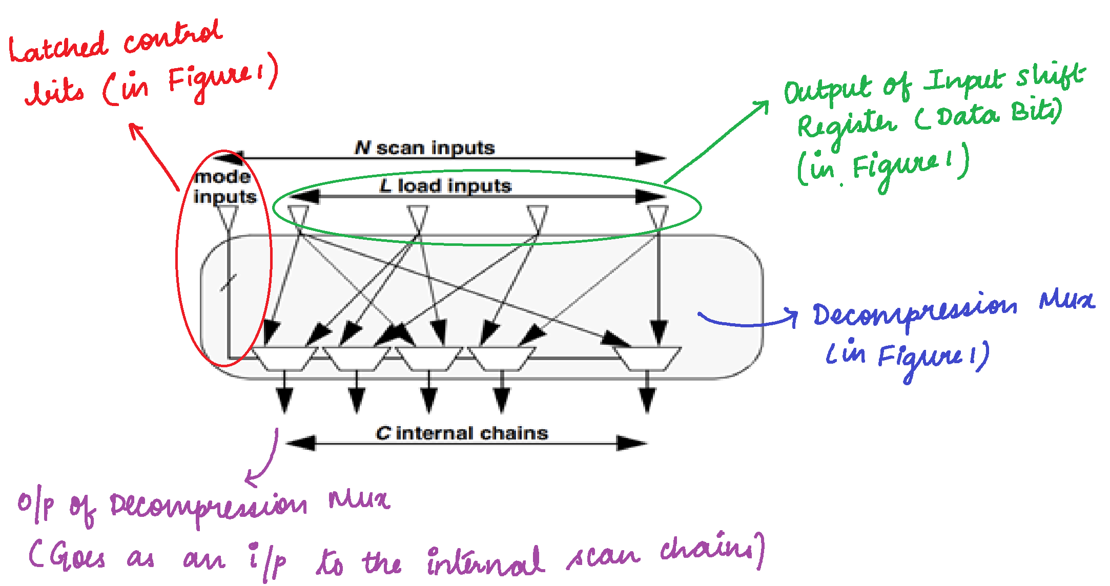
We will try to correlate Figure 5 with Figure 1 using the Figure 6
Figure 6 : Correlating Figure 5 with Figure 1
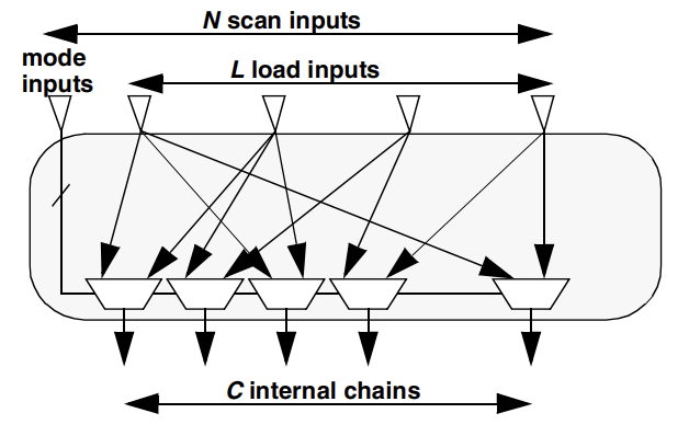
The load decompressor can be obtained by connecting chains (i.e., C internal chains in the above figure) to inputs (i.e., L load inputs in the above figure).
By construction, any two chains connect to different inputs in at least one mode.
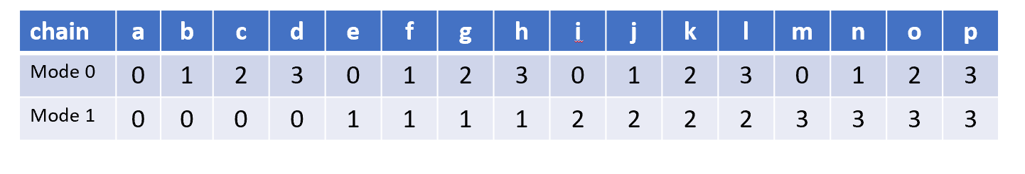
For example, for M = 2 modes (mode 0 and mode 1), L = 4 load inputs (0, 1, 2, 3), C = 16 chains (a, b,..., p) can be connected as shown below,
Figure 7 : Connecting chains to inputs
For example, chain c connects to input 2 in mode 0 and to input 0 in mode 1 (as shown in the above figure).
Note that chains a, f, k and p connect to the same input in both modes, thus do not require a MUX.
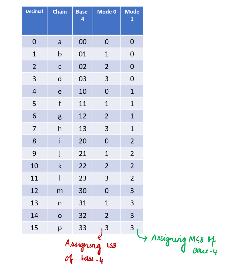
Let’s explore how to arrive at the table shown in Figure 7.
The table is arrived using a systematic numbering method based on : L = 4 → number of scan inputs (indexed as 0, 1, 2, 3)
M = 2 → number of control modes (mode 0 and mode 1)
C = 16 → number of scan chains
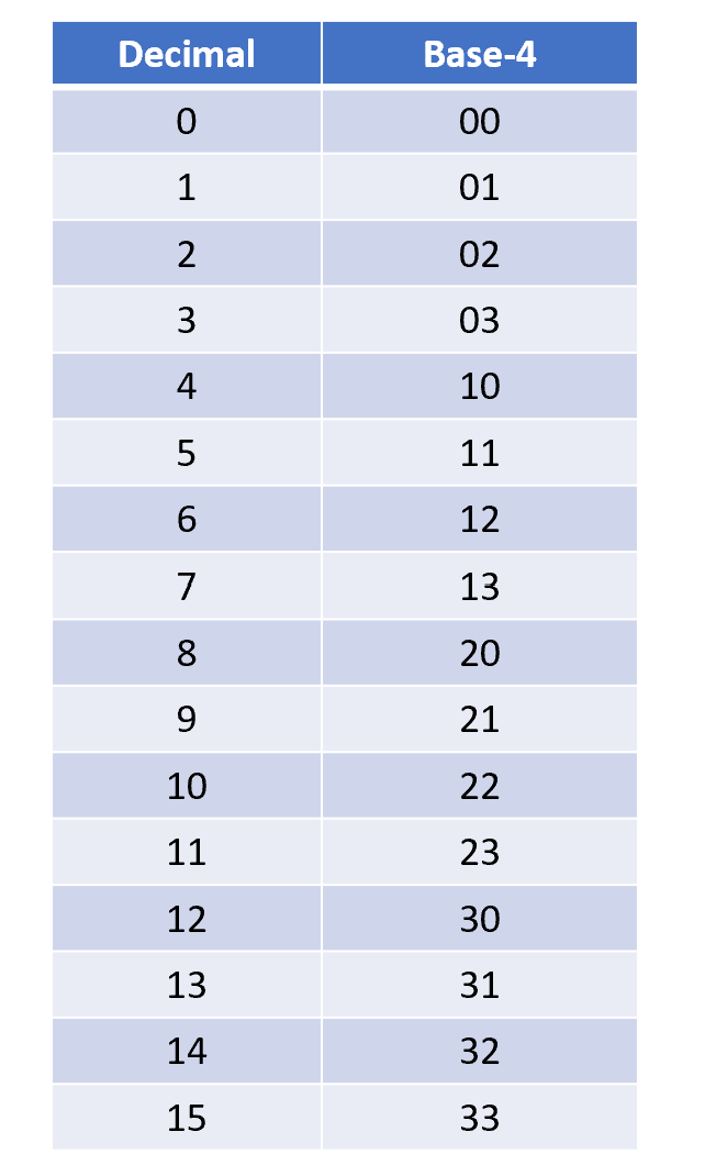
Each scan chain is assigned a unique 2-digit number in base 4 (radix L).
Figure 8 : Decimal to Base-4 Conversion Table
Figure 9 : Explains the logic used to generate the scan chain mapping table presented in Figure 7
Control Register
The control register is a bank of latch cells that stores the configuration of the scan circuit for a given pattern.
Some of the register bits control the mapping of input shift-register bits to scan chains through the decompression MUX, while others control the X-masking logic at the ends of the scan chains.
In this example (Figure 1), two bits control the decompression MUX and two bits control the X-masking logic. The control register latches remain constant during scan shifting, so the scan configuration stays the same within a given pattern. (i.e., in Figure 1, two latched control bits goes to Decompressor Mux and two latched control bits goes to X-masking logic at the ends of scan chains)
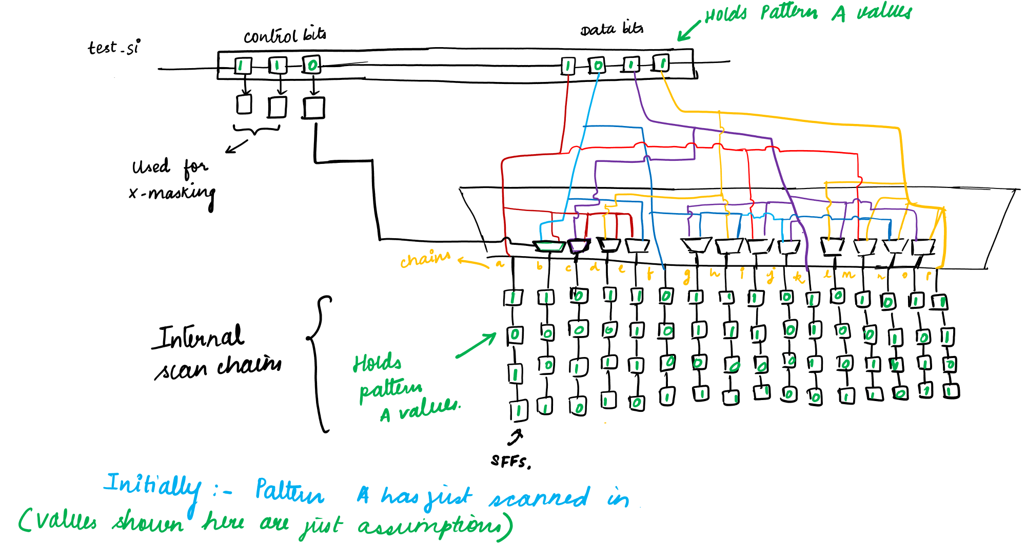
Illustration
Let’s visualize the above mentioned points using the following illustration.
< < The illustration provided here is intended to aid in visualizing the concept. Please note that it may not represent the process with complete accuracy, as I am still in the process of learning and refining my understanding > >
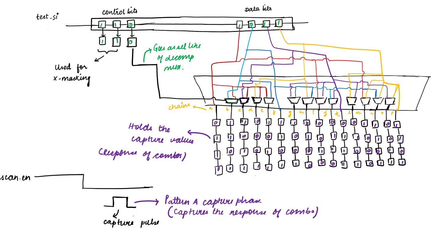
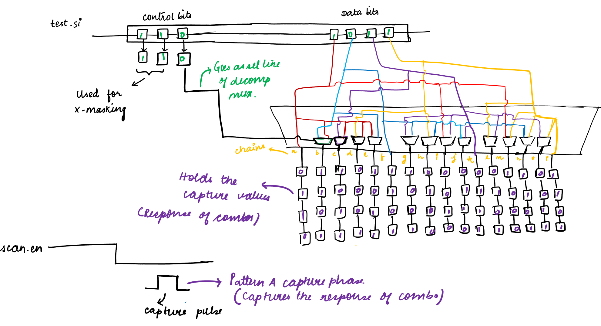
Consider two consecutive test patterns, A and B, starting from the point at which pattern A has just been scanned in.
Initially,
< < Note : The decompressor mux structure is drawn by considering the connections given in Figure 7. The configurations used in this illustration are not related to Figure 1 > >
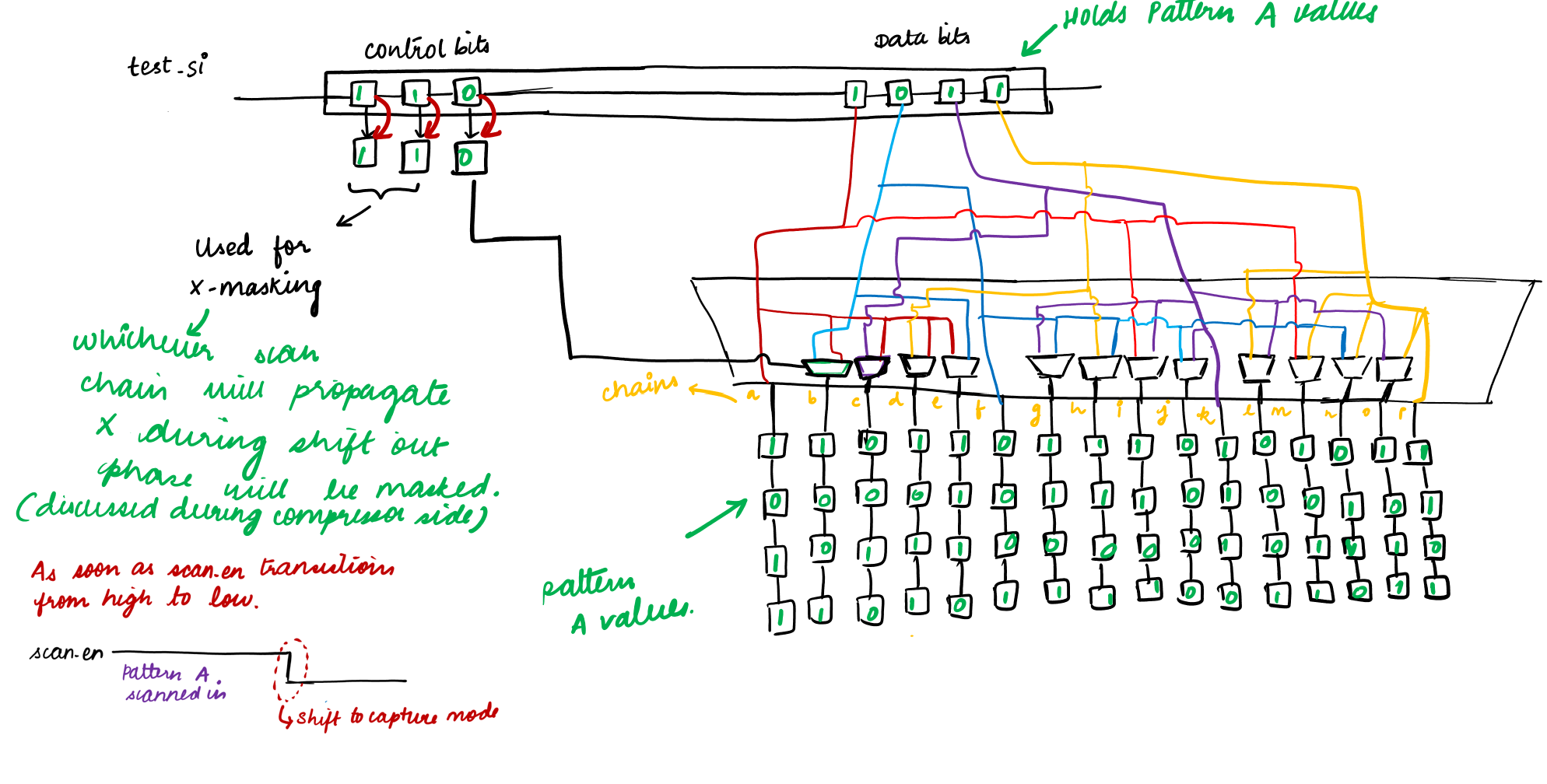
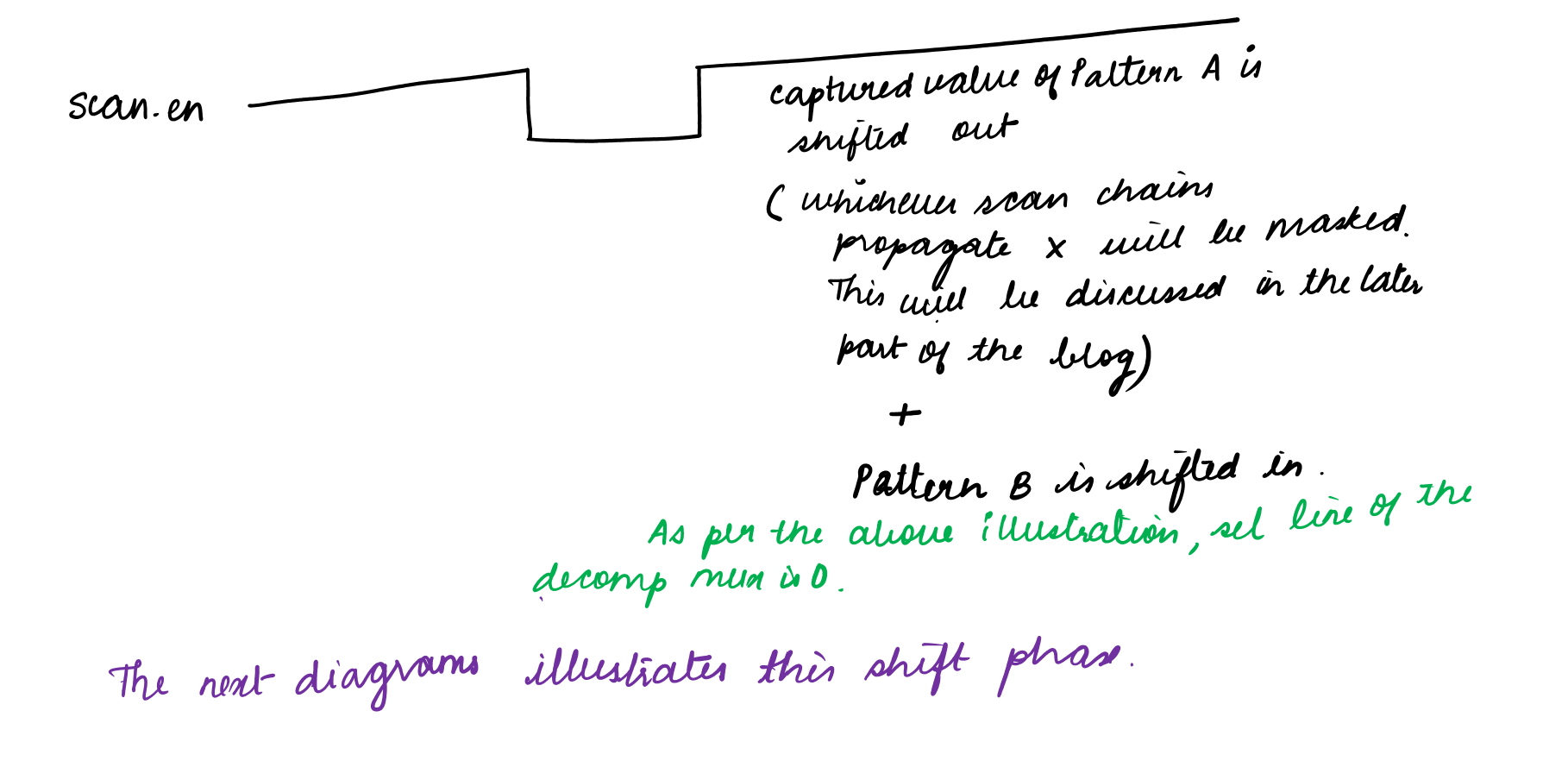
When the scan-enable signal changes from high to low,
The de-assertion of the scan-enable (test_se) pin performs the following :
It latches the three control bits from the input shift register into the control register latches. This configures the X-masking circuit to scan out the data from pattern A, and it configures the decompression MUX to decompress the data for incoming pattern B.
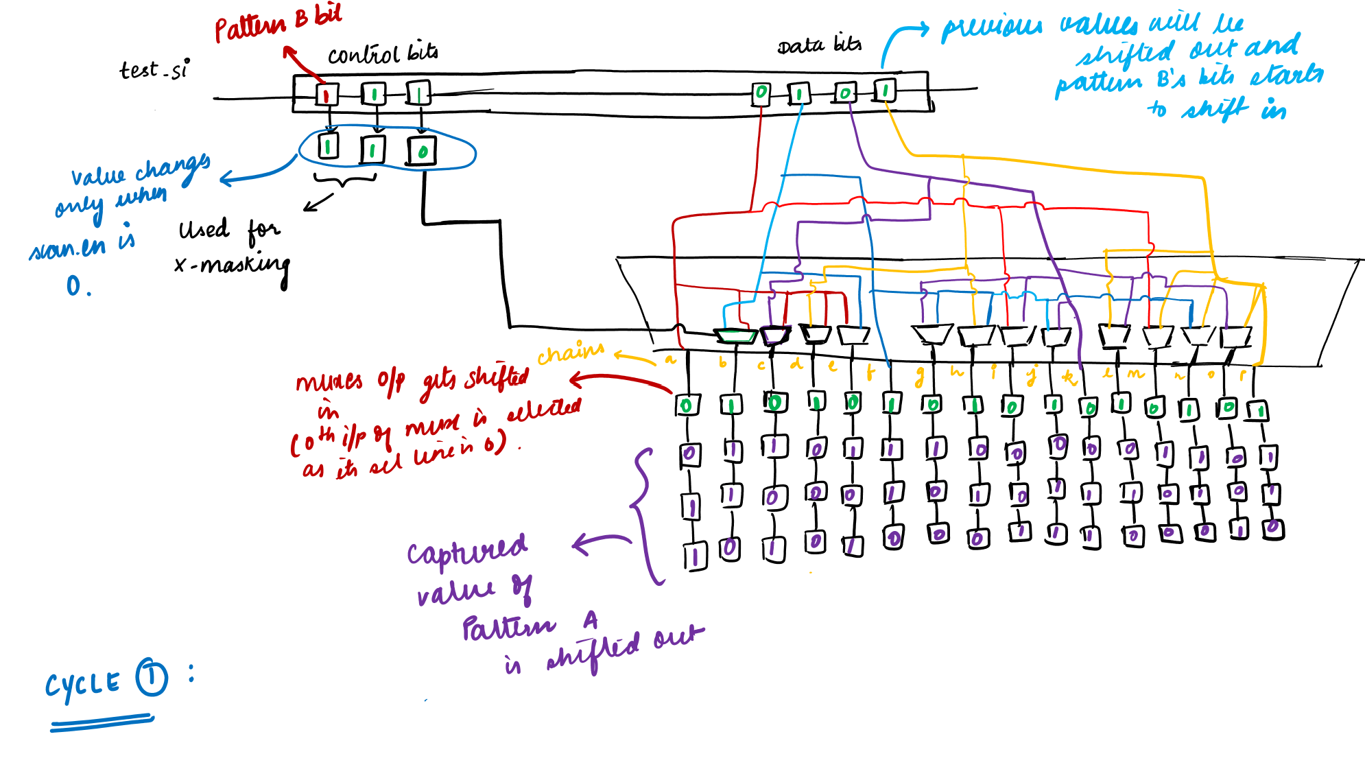
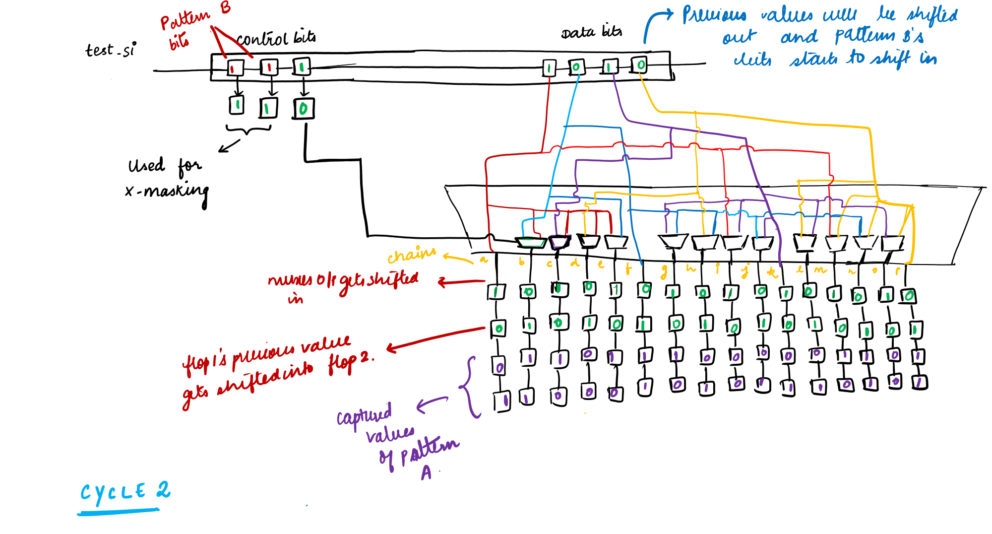
When capture pulse is pulsed,
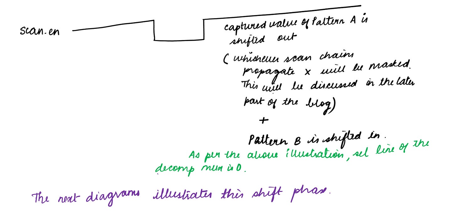
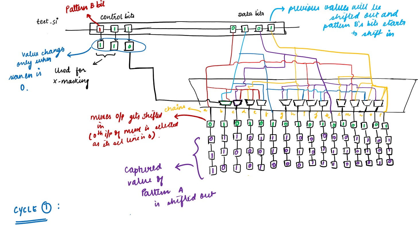
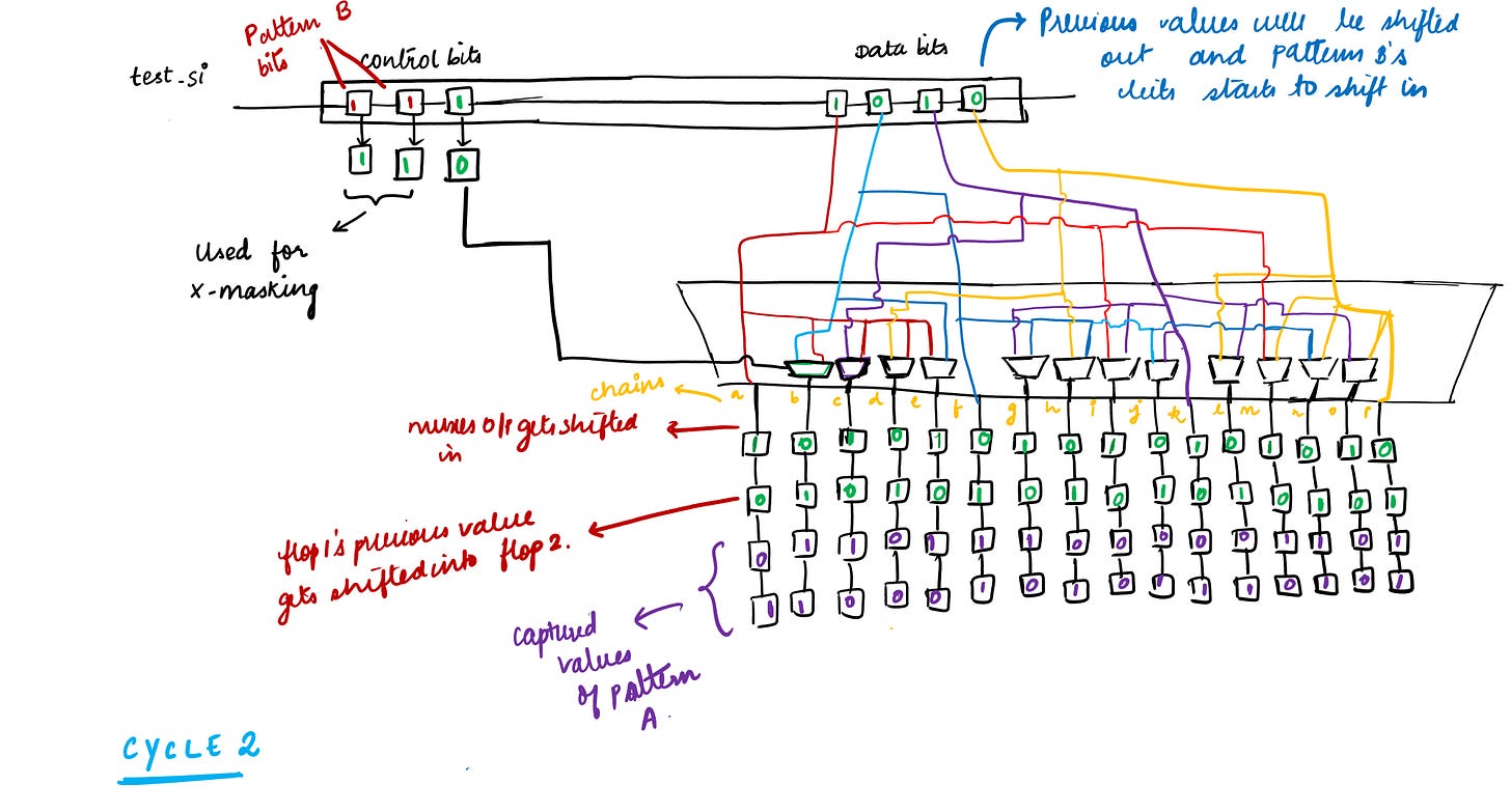
The same process repeats till captured value of Pattern A is shifted in and Pattern B’s bits gets shifted in.
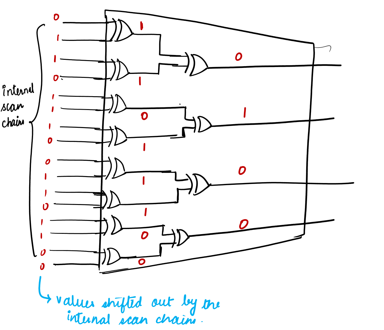
Output XOR Compression Tree
Compressor compresses the values shifted out by the internal scan chains.
The XOR compression tree is a multilevel combinational network of XOR gates that compresses the output bits from the scan chains into a smaller number of bits
Figure 10 : Explains the working of compressor
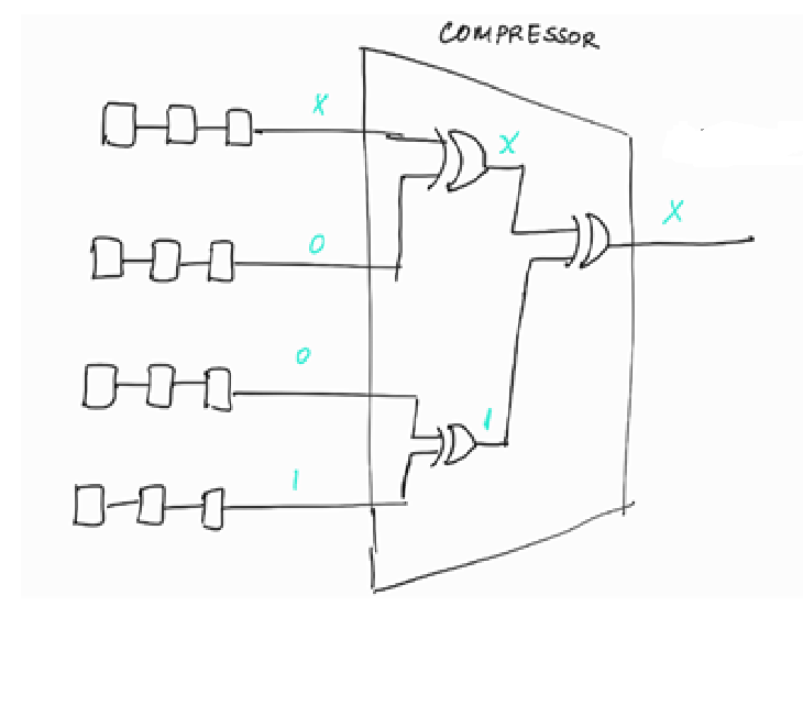
Problem in Compressor Logic
X propagation.
Figure 11: X propagation in Compressor
As seen in the figure above, the propagation of an unknown value (X) on one scan chain prevents the observation of values on the other scan chains.
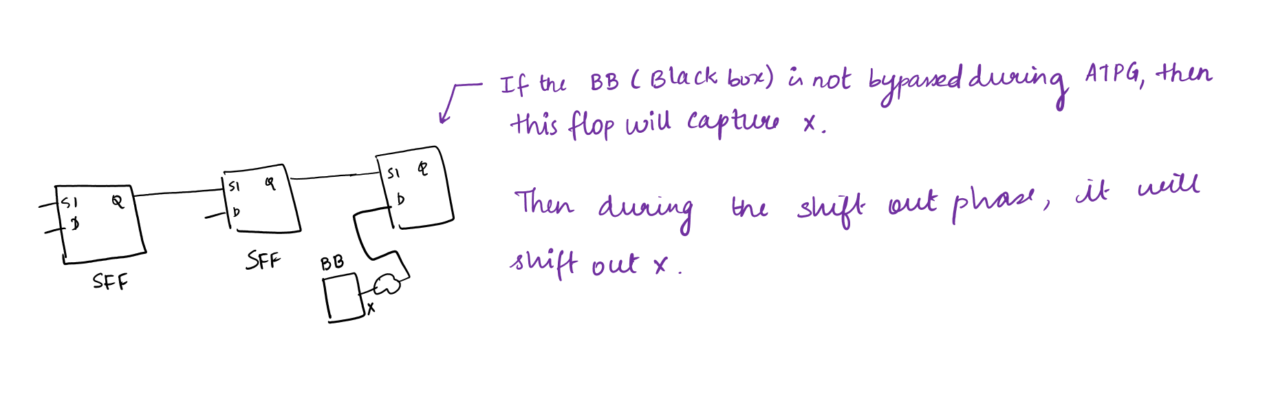
Why do scan chains propagate X ?
If there are any Black Boxes in the design, it’s output will be X. Black Boxes have to be bypassed during ATPG to stop the propagation of X. If Black Boxes are not bypassed during ATPG, then X will be propagated to the downstream logic and the flop will capture X (as depicted in the below figure) The captured value of the flop will be shifted out during shift out phase. So scan chains will propagate X.
Figure 12 : Why do scan chains propagate X?
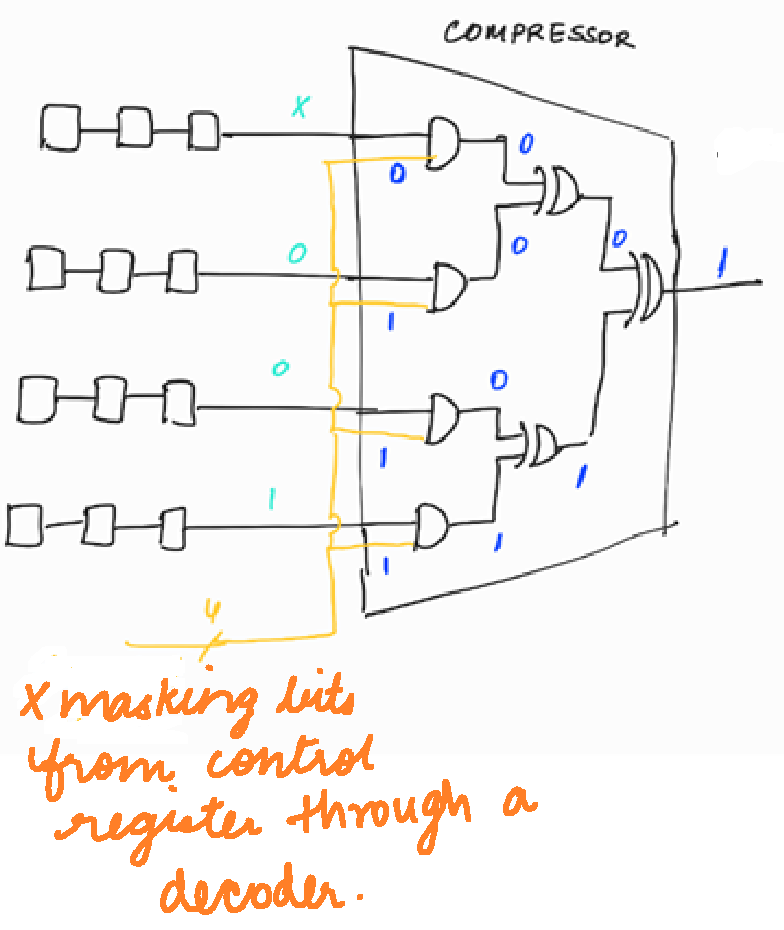
How to stop the propagation of X? To stop the propagation of X, the masking logic is used. Masking logic will mask the scan chains that is propagating X.
Figure 13 : X-masking
While doing fault simulation, the TestMAX ATPG tool will come to know which all logics will capture X. So the tool will write a pattern in such a way that the scan chain which is propagating X will be masked.
< < Note : Fault simulation is a process used by ATPG tool to generate test patterns > >
The X-masking bits from the control register specify the chain or chains to mask for the current pattern.
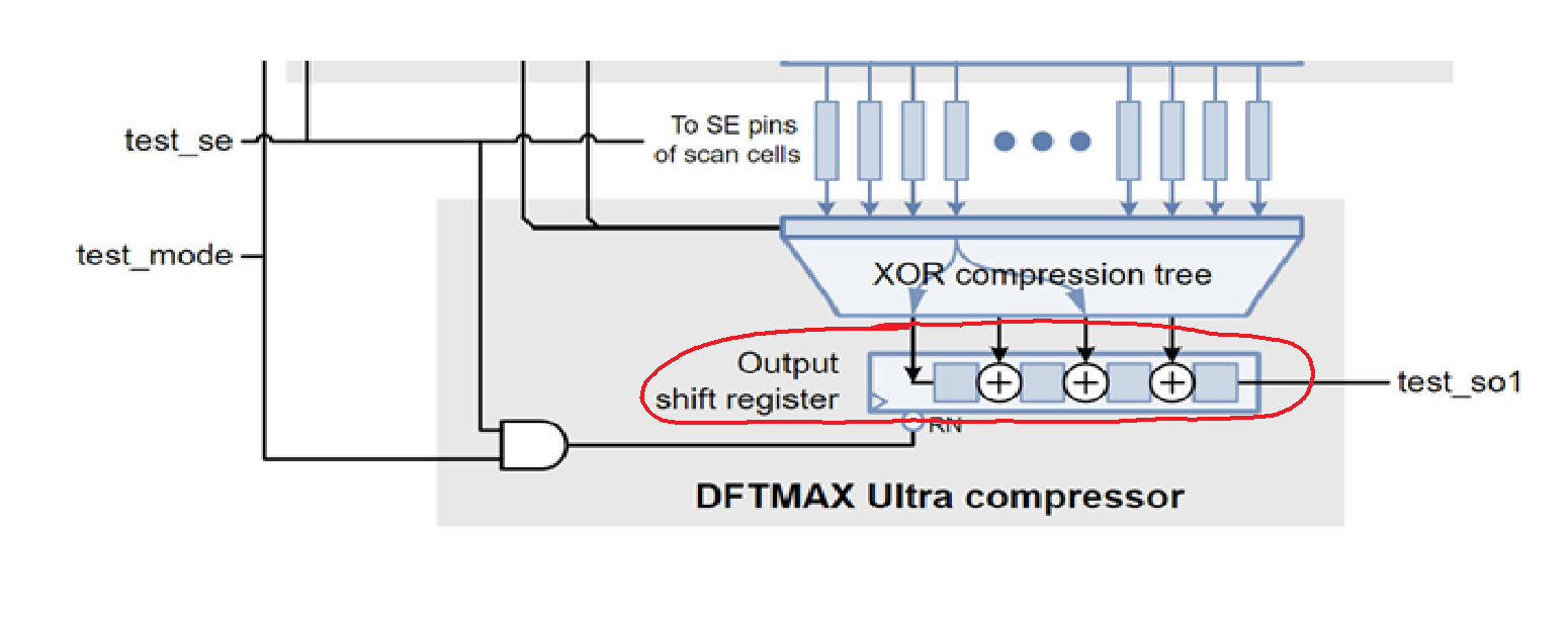
Shift Register at the Output :
Figure 14: Output XOR tree and Shift Register
The compressed bits feed into a chain of flip-flops that operate as an output shift register, which is clocked on the leading clock edge at the normal scan clock rate. During scan capture, the register is reset by the scan-enable signal (i.e., during capture scan-enable = 0, RN of the flops = 0, as shown in the above figure). During scan shift, the XOR gate between each stage of the shift register merges scan data from an XOR compressor output into the scan data already moving through the output shift register. This architecture further compresses the scan data outputs from the XOR compression tree into a single data stream.
Test Pattern Scan Procedure
< < Please use figure 1 as the reference figure > >
The ATE equipment performs the scan-in, scan-out procedure as specified by TestMAX ATPG.
Consider two consecutive test patterns, A and B, starting from the point at which pattern A has just been scanned in :
The first four bits of the input shift register (shifted in at the end of pattern A) contain the desired scan control bits to be latched into the control register.
The scan-enable signal test_se changes from high to low, transitioning the device from scan shift mode to scan capture mode.
The de-assertion of the test_se pin performs the following:
o It latches the four control bits from the input shift register into the control register latches. This configures the X-masking circuit to scan out the data from pattern A, and it configures the decompression MUX to decompress the data for incoming pattern B.
o It resets the output XOR shift register to known zero values.
A clock pulse applied to the clock input causes the capture event, which changes the contents of the scan flip-flops (captures the response of the combo logic)
The scan-enable signal test_se is asserted, which transitions the device from scan capture mode back into scan shift mode.
The ATE equipment applies a sequence of clock pulses at the scan clock rate. This reads out the captured scan data for pattern A through the test_so1 output and, at the same time, scans in the data for pattern B through the test_si1 input.
Scan-in and scan-out continue until the scan chains are filled with the data for pattern B (and the first four bits of the input shift register are filled with the control bits for the next pattern)


Thank you.
Sure I will make a series on IJTAG
Please continue the series..