


Why DFT (Design For Testability) ?
DFT Basics: Article #1


Welcome to my blog, where we explore the fascinating world of VLSI design. Dive into topics like essential steps in ASIC flow, Design for Testability, critical role of testing in modern semiconductor technology. Discover why DFT is indispensable for ensuring reliable, high-quality chip designs.
VLSI ASIC Design - The Art of Miniaturizing Complexity
VLSI (Very Large Scale Integration) involves the fabrication of million transistors in small area, enabling powerful, compact, and efficient electronic device.
An ASIC (Application Specific Integrated Circuit) is an integrated circuit (IC) that's custom-designed for a particular task or application. For instance, a Modem chip can’t be used as a chip which is used for deployment of airbags in automobiles
Key Goals of VLSI ASIC Design:
High Performance: Ensuring faster processing.
Low Power Consumption: Optimizing power usage to extend battery life.
Minimal Area: Reducing chip size to achieve compact products.
ASIC Design Flow: A Step-by-Step Guide
Designing an ASIC is a complex process that involves several stages to ensure the final chip meets its intended specifications. Here’s an overview of the key steps in the ASIC design flow:

Design Specification :
Based on the application for which we are designing the chip, certain specifications like what has to be the speed, how many memory modules, processors, sensors are required, what has to be the power etc. will be decided.
Design Code :
Design Team will write the design code of the chip. They describe the functionality of the chip.
Design Team write in behavioral model, dataflow level model because it is easier to describe the functionality of the chip.
Verification :
It is to validate the functionality of the design to ensure that it meets the required specifications and performs as indented.
Synthesis :
The behavioral and dataflow level model code is converted into structural form (or) technology node specific gate-level netlist.
If we want to go for low power design, then certain special cells like clock gating cell, isolation cells, retention registers etc. will also be inserted.
Design For Testability (DFT) :
DFT is to insert test structures in the design during the pre-silicon stage to facilitate detection of manufacturing defects in a chip.
Physical Design (PD) :
The gate level netlist is converted into layout form.
Sign Off :
Static Timing Analysis (STA) : It is a method of validating the timing performance of a design by checking all possible paths for timing violations.
Physical Verification (PV) : It is to verify the layout of circuits.
Logical Equivalence Checks (LEC) : Our design undergoes a lot of changes in each stage. So LEC is done to check whether the final design is logically equivalent to the original design.
LEC will be performed after every step (i.e., after synthesis, after DFT insertions, after PD)
Tape Out :
Delivering the database to the manufacturing unit.
Packaging and Testing (After manufacturing) :

Covering the Die with a protective layer is called Packaging.
Testing is to check whether our chip is good or not (i.e., to check whether our chip has any manufacturing defect or not)
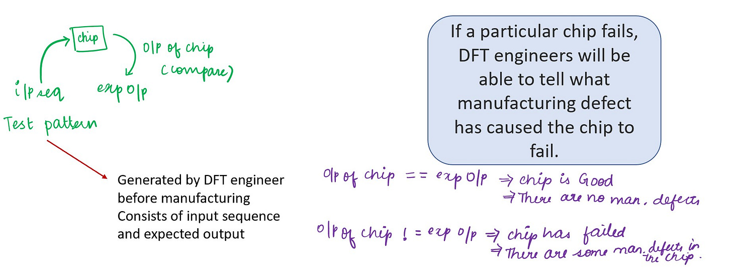
Design For Testability (DFT) :
DFT involves inserting test structures in the design (like scan insertion, MBIST insertion, Boundary Scan insertion) during the pre-silicon stage to facilitate detection of manufacturing defects in a chip.
If a particular chip fails after manufacturing, DFT team will be able to tell what manufacturing defect has caused the chip to fail.
What are manufacturing defects?
Defects that are caused due to
Process Variations : Slight variation in transistor channel length, metal interconnect width and thickness etc. will impact the logical and timing performance.
Random Imperfections : Results in unintentional shorts, unintentional opens etc.
What is Testing?
(Done after manufacturing)
Testing is a process of determining whether a device is good or not (i.e., whether our chip has any manufacturing defect or not).
Testing includes test pattern generation, application and output evaluation.

Role of a DFT Engineer :
DFT engineers play a critical role in the semiconductor industry, but their focus is different from that of the Functional Verification team.
While Functional Verification engineers ensure that the chip works as intended (i.e., they validate the functionality), DFT engineers ensure the quality of the chip by identifying manufacturing defects. Let’s explore why DFT is essential, even when a Functional Verification team is already in place.
Why do we need DFT team when we have Functional Verification Team?
Consider the following example:
Design:
A 10-bit counter with:
Counter initialization circuit
Counter observation logic
Scenario:
Suppose the counter has a manufacturing defect. After counting to 999, instead of incrementing to 1000, it incorrectly rolls back to 999.
If Only the Functional Verification Team Exists:
The counter is manufactured with a defect. So after counting to 999, instead of incrementing to 1000, it incorrectly rolls back to 999.
The Functional Verification team tests the counter using functional patterns.
In this example, it will take more than 1000 clock pulses to tell that the counter is failing.
Reason : Functional Verification engineer check the functionality i.e., they check if the counter counts from 0 to 1023 properly. The counter is failing at the 1000th pulse (i.e., at the 1000 pulse, counter is again counting 999 instead of 1000). So 1000 pulses are required. Some more clock pulses are required for counter initialization and counter observation. So Functional Verification team require more than 1000 clock pulses to tell that the counter is failing.
Functional Verification team can only tell that the counter is failing.
Reason : Functional Verification engineer check the functionality i.e., they check if the counter counts from 0 to 1023 properly or not. In this case, after counting to 999, instead of incrementing to 1000, it incorrectly rolls back to 999. So the counter is failing.
If a DFT Team Exists:
The counter is manufactured with a defect. So after counting to 999, instead of incrementing to 1000, it incorrectly rolls back to 999.
DFT patterns are used to test the chip.
DFT team will be able to tell that the counter is failing approximately in the range of 100 clock pulses. DFT team require less no. of clock pulses to tell that the counter is failing compared to functional verification team. So Test time will be less compared to functional verification team.
Reason : DFT team go for scan insertions. So we will be easily able to control and observe our design.
< < We will discuss about this in detail during scan insertion topic > >
DFT team will be able to tell that the counter is failing and also tell what manufacturing defect has caused the counter to fail.
Reason : DFT patterns are generated using ATPG. ATPG tool does fault simulation to generate the test patterns. During fault simulation, ATPG tool mimics all possible failure situations that might occur after manufacturing and it tries to find a pattern that will be able to detect that particular failure situation, if suppose it occurs after manufacturing. Those patterns will be written in the final pattern list. These test patterns will be used to test the chip after manufacturing. As we are doing fault simulation to generate the patterns, if a particular pattern fails, we will be able to tell the possible causes of failures.
< < We will discuss about fault simulation in detail during ATPG topic > >
Conclusion
With DFT patterns, the test time will be less compared to functional patterns.
DFT will be able to tell what manufacturing defect has caused the chip to fail.
As DFT patterns has these advantages over functional patterns, DFT patterns will be used to test the chip after manufacturing.
Some functional patterns will also be used to test the chip after manufacturing.
If DFT patterns are used to test the chip after manufacturing, why do we need functional verification team?
Consider the following example :

In the above example, even though there are no manufacturing defects, the circuit will not function like half adder.
Why ?
Because the design itself was wrong.
This is the signification of functional verification team. They validate the functionality.
i.e., they check whether the below code is correct or not.
sum = a xor b;
carry = ab ;
Design for Testability (DFT) is an essential aspect of modern VLSI design. It ensures that complex chips can be effectively tested for manufacturing defects.
Thank you for sharing vidisha