Scan DRC (part 2)
DFT Basics Article #6


In my previous blog DFT Basics: Article 5 , we gained an understanding of clock controllability and set/reset controllability Design Rule Checks (DRCs), which are essential for ensuring proper scan chain functionality.
In this blog, we will dive deeper into other Scan DRCs, such as feedback loop DRC, X-source DRC, potential race condition DRC, and bus contention DRC.
Feedback Loop DRC

Due to the feedback, the output is continuously oscillating.
Thus the ATPG tool can’t determine whether the net is 0 or 1. So it will consider it as X.
If suppose for detecting some faults, if this combination of inputs is required, then because of the feedback, those faults will not get detected.


X Source DRC
X source is a logic whose output is X.
Reason 1:
If there are any memories or analog blocks (Example RF), the ATPG tool will consider the output as X. As a result, X will be propagated to the downstream logic which is connected to the output of memories/analog blocks.
This will result in coverage drop during ATPG
< < We will explore about this in detail during ATPG topic > >

So we need to bypass the memories and analog blocks.
Memories will be tested using MBIST and analog blocks will be tested with different methods.
Bypassing the memories and analog blocks
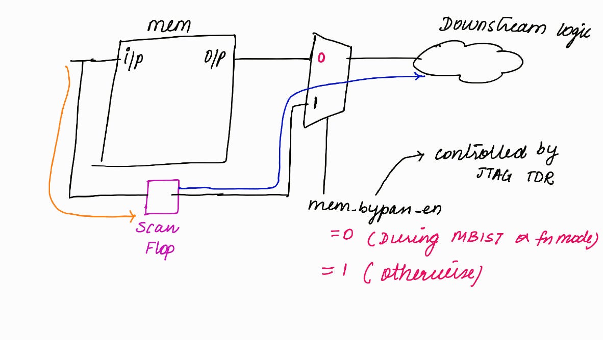
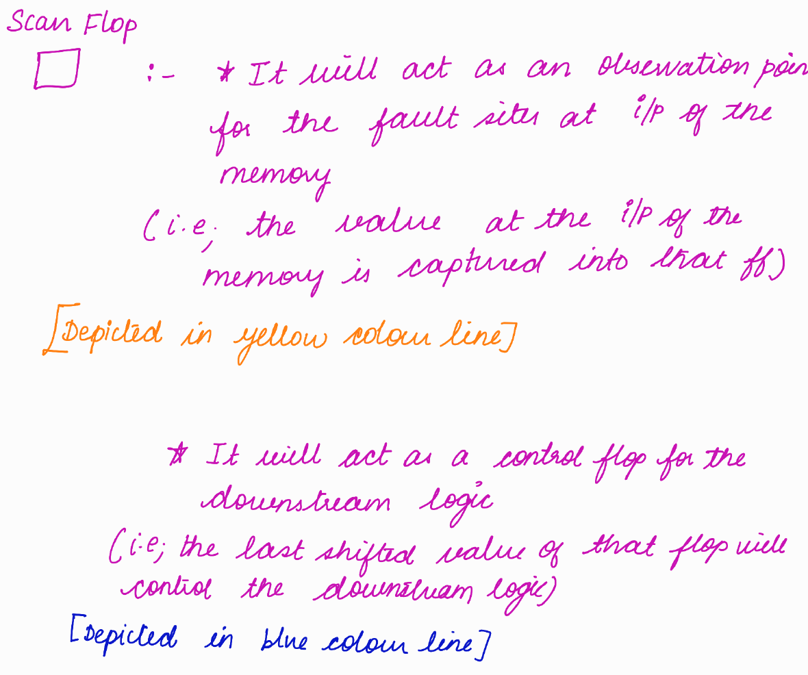
There will be a .tcd_mem_lib file for each memory model.
In the .tcd_mem_lib, if the Transparent Mode option is given as SyncMux, the tool will automatically add the memory bypassing logic which is shown in the above picture.
The analog blocks will be bypassed by the designer.
Reason 2:
If the module definition of a particular module is not available, then you can black box that module.
As we have black boxed that module, it’s output will be X.
So X will be propagated to the downstream logic which will result in coverage drop during ATPG.
So we need to bypass the black box.
Mostly try to get the module definition of all the modules from functional team and read it. Otherwise the particular module will not be tested.
Potential race DRC
Clock Data Race Condition
Set/Reset Race Condition
Clock Data Race Condition
If the clock signal goes to the clock port and the D port.
This will cause problem during DFT mode. The flop will capture the same value during all the capture phases which will result in coverage drop during TDF ATPG runs.
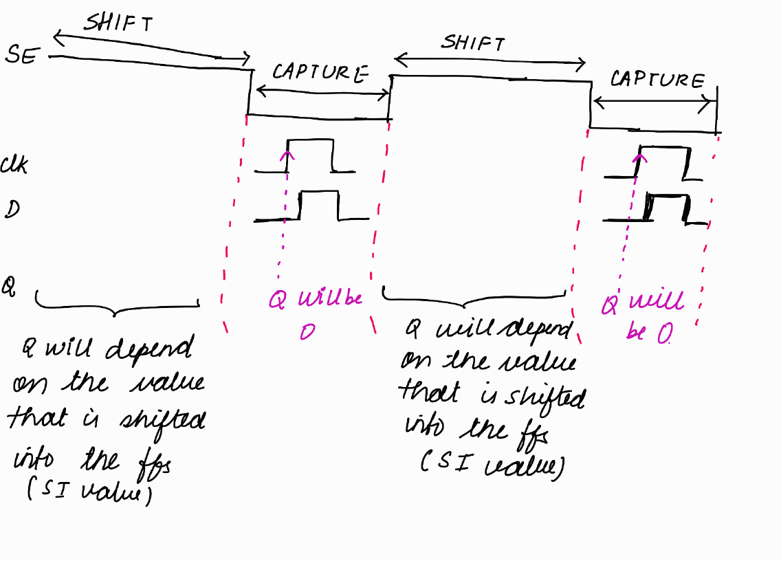
If clock signal reaches clock port at a slightly earlier time, the flop will capture ‘0’ during all the capture phases.
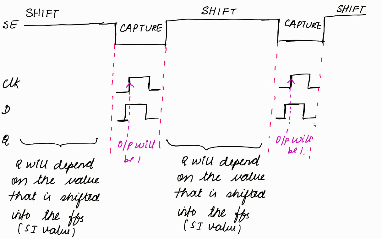
If clock signal reaches D port at a slightly earlier time, the flop will capture ‘1’ during all the capture phases.
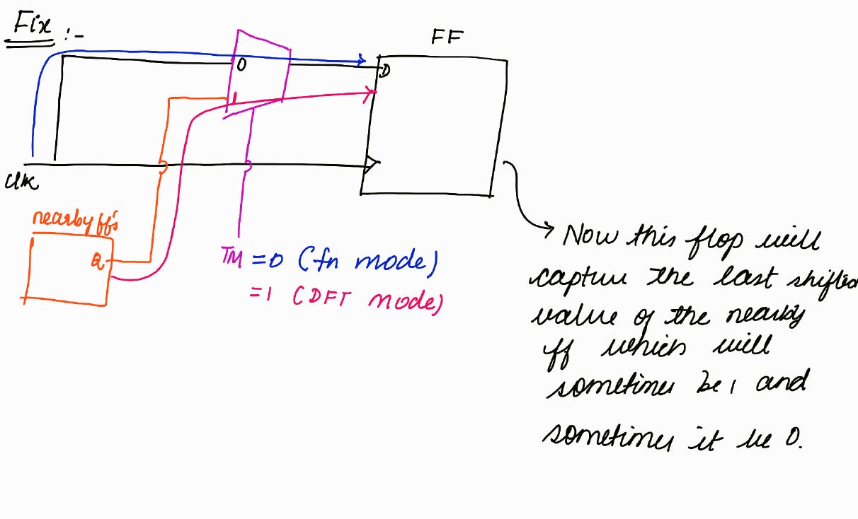
We need to fix the DRC in such a way that the functionality is also not affected but at the same time, we will overcome the problem caused during DFT mode.
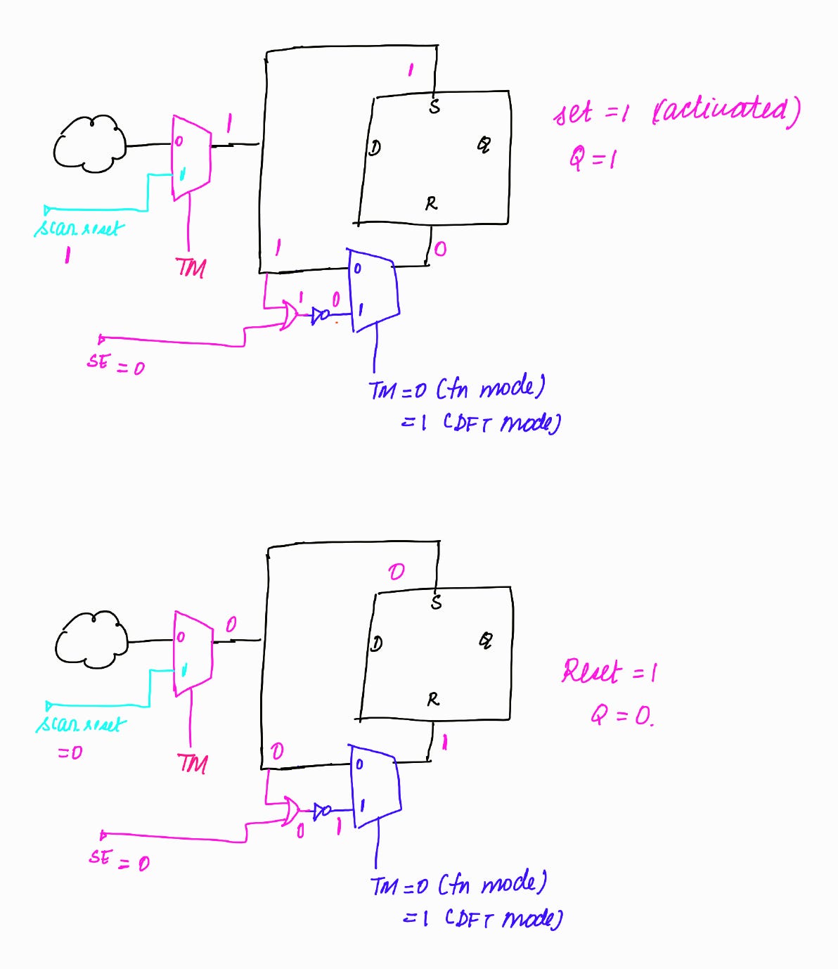
Set/Reset Race condition
If the same signal is controlling both the set and reset port of the flop.
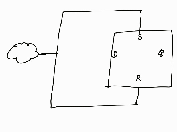
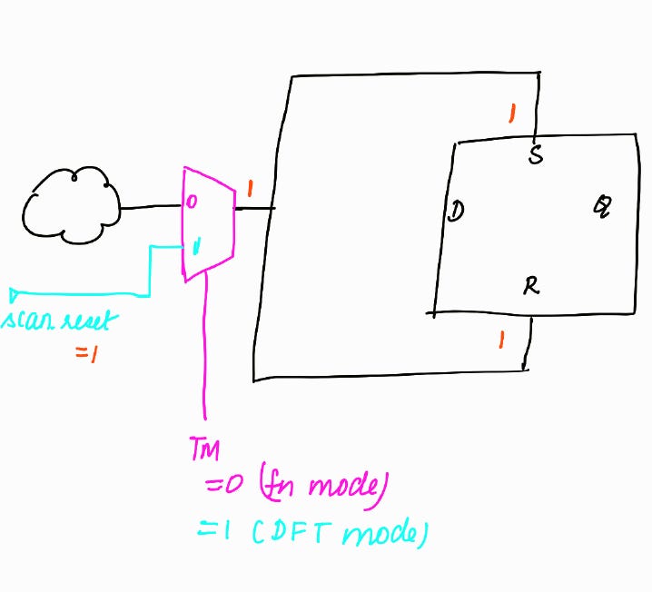
There is a confusion of whether the flop has to set (Q= 1) or reset (Q= 0).
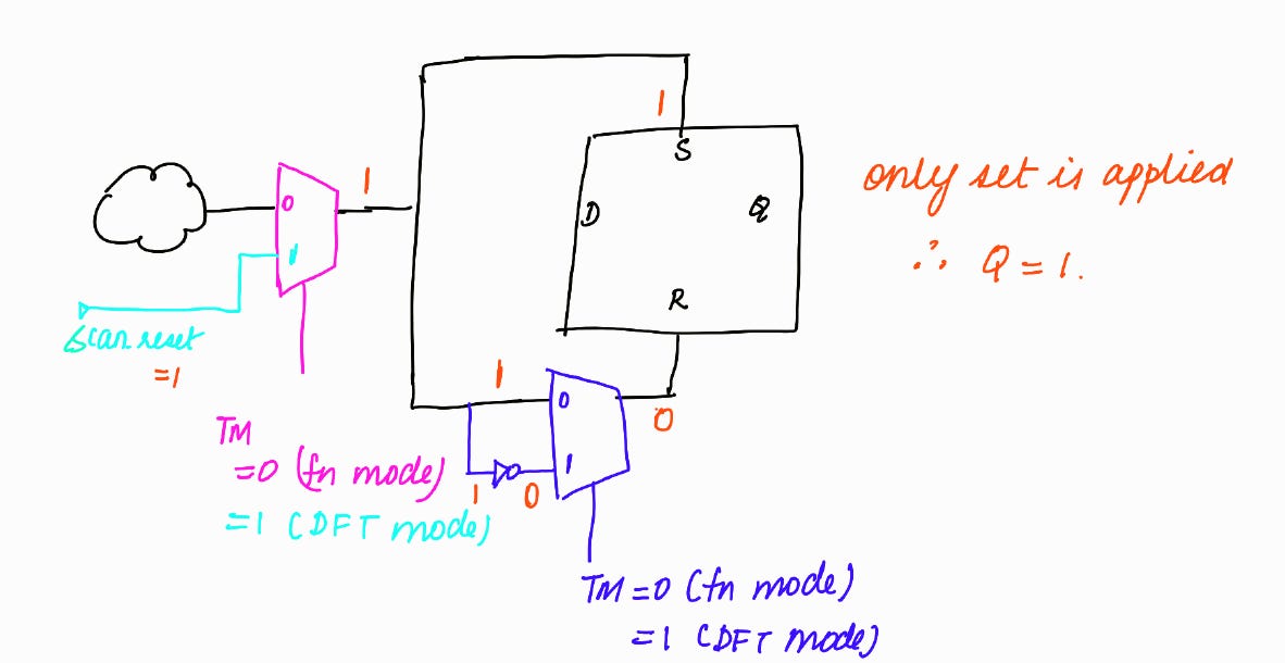
This is a design problem. We can temporarily make the fix in the DFT mode.
But there is still a problem with the above fix.
During shift, scan_reset will be 0 (off state)
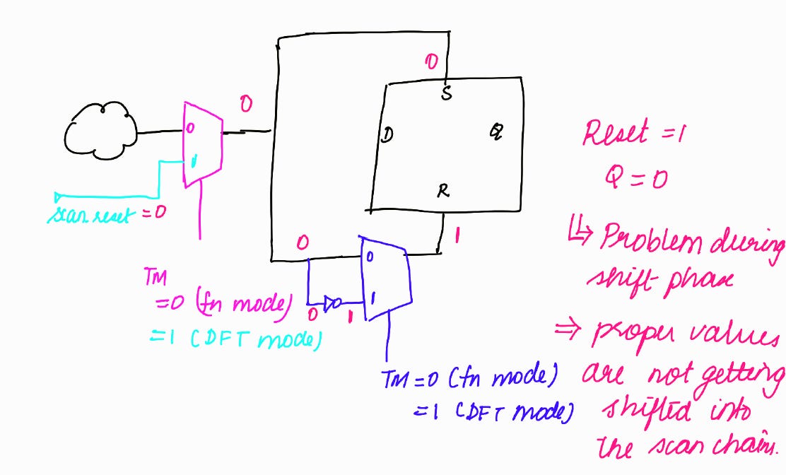
< < We had explored in the previous blog DFT Basics :Article#5 of what will happen if the flop goes into the reset state during shift >>
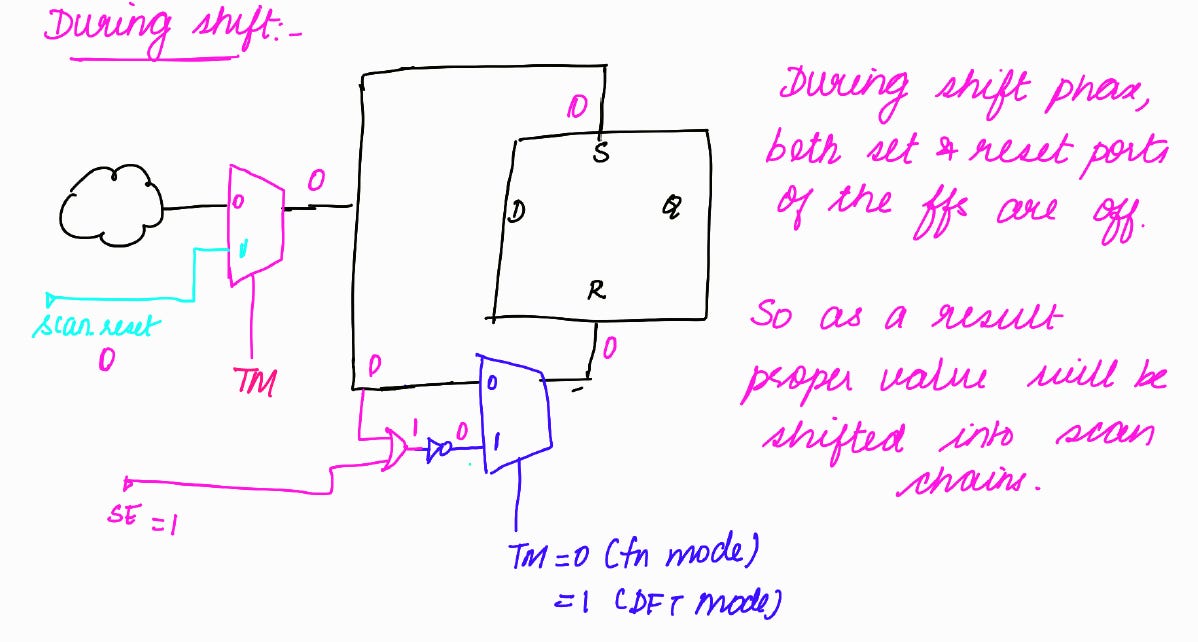
If you declare reset as a clock (i.e., using add_clocks command in Tessent Scan tool), in shift phase, the tool will always keep the reset in its off state.
During Shift :
If you declare reset as a clock (i.e., using add_clocks command in Tessent Scan tool), in capture phase, for some patterns, tool will activate the reset. For some patterns, it will not activate the reset.
During Capture :
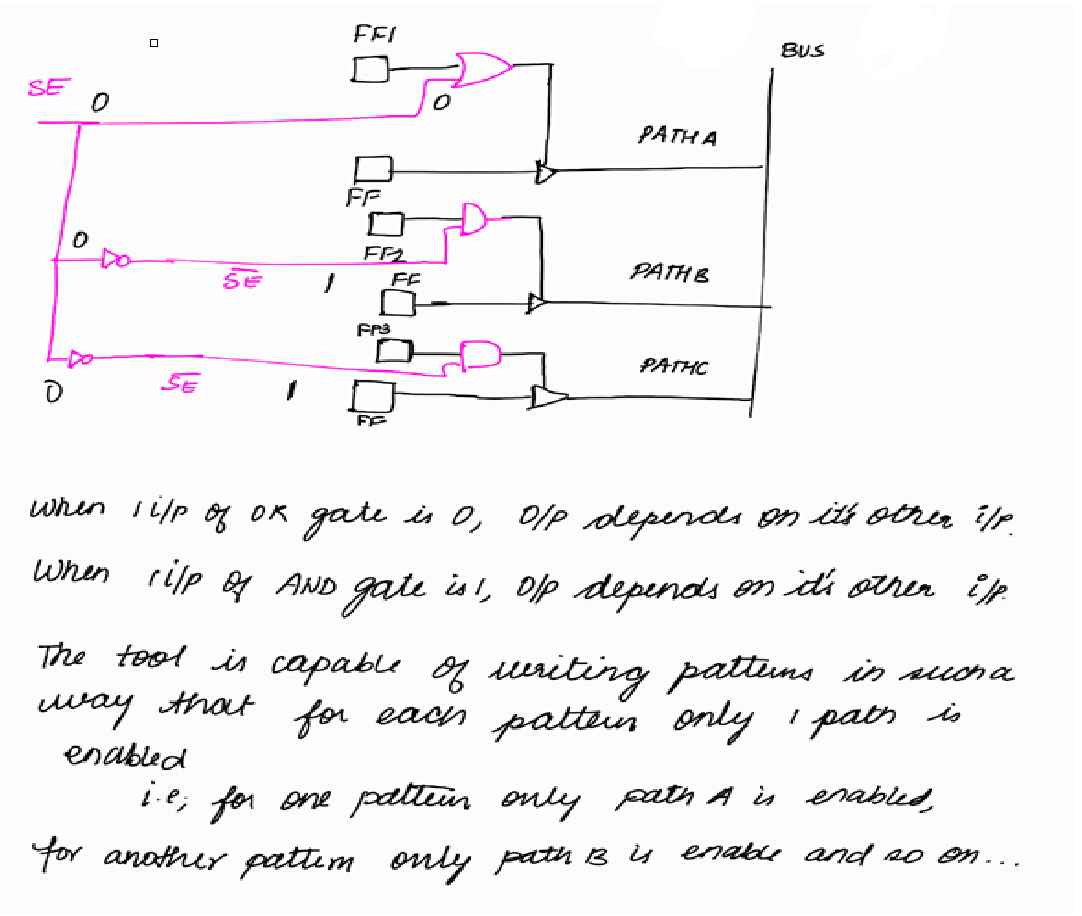
BUS-CONTENTION DRC
Bus contention occurs when 2 or more bus drivers force opposite values onto a bus.
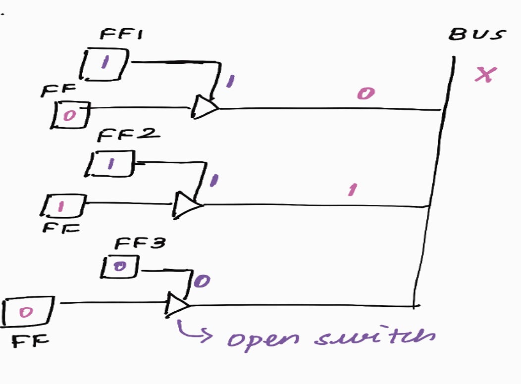
Bus contention is designed not to happen during normal operation (functional mode) (it is taken care by designer) and it is typically avoided during capture operation (it is taken care by DFT tool). During shift, no such guarantee can be made.
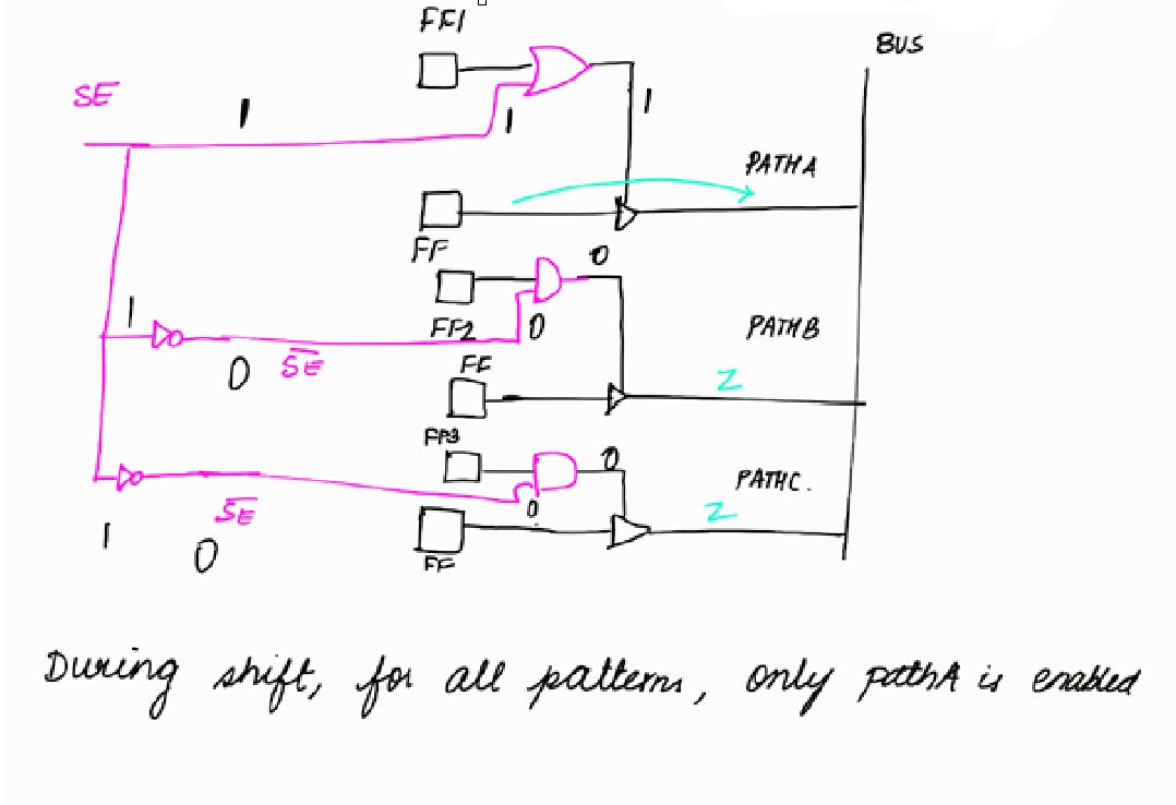
Fix :
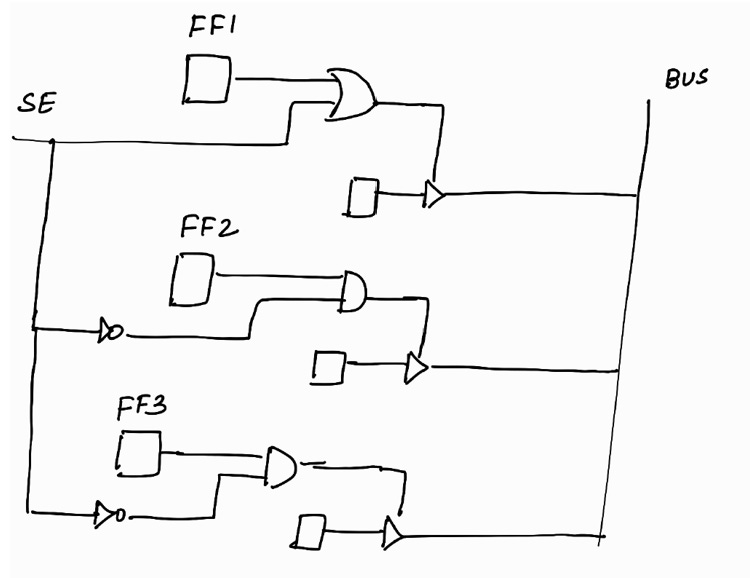
During Shift :
During Capture :