
Scan Insertion
DFT Basics : Article #2


In my previous blog DFT Basics : Article #1, we explored VLSI design and the significance of Design for Testability (DFT) in ensuring high-quality, defect-free chips. We discussed why DFT is indispensable in modern semiconductor design.
Building on that foundation, this article explores Scan Insertion, a fundamental DFT technique that transforms design into a testable structure. We will explore its process, and how scan chains operate.
Let's get started!
What is scan insertion?
All the flops will be converted into scan flops and the scan flops will be stitched into scan chains.
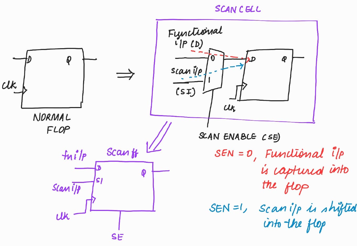
Normal flops converted into Scan Flops
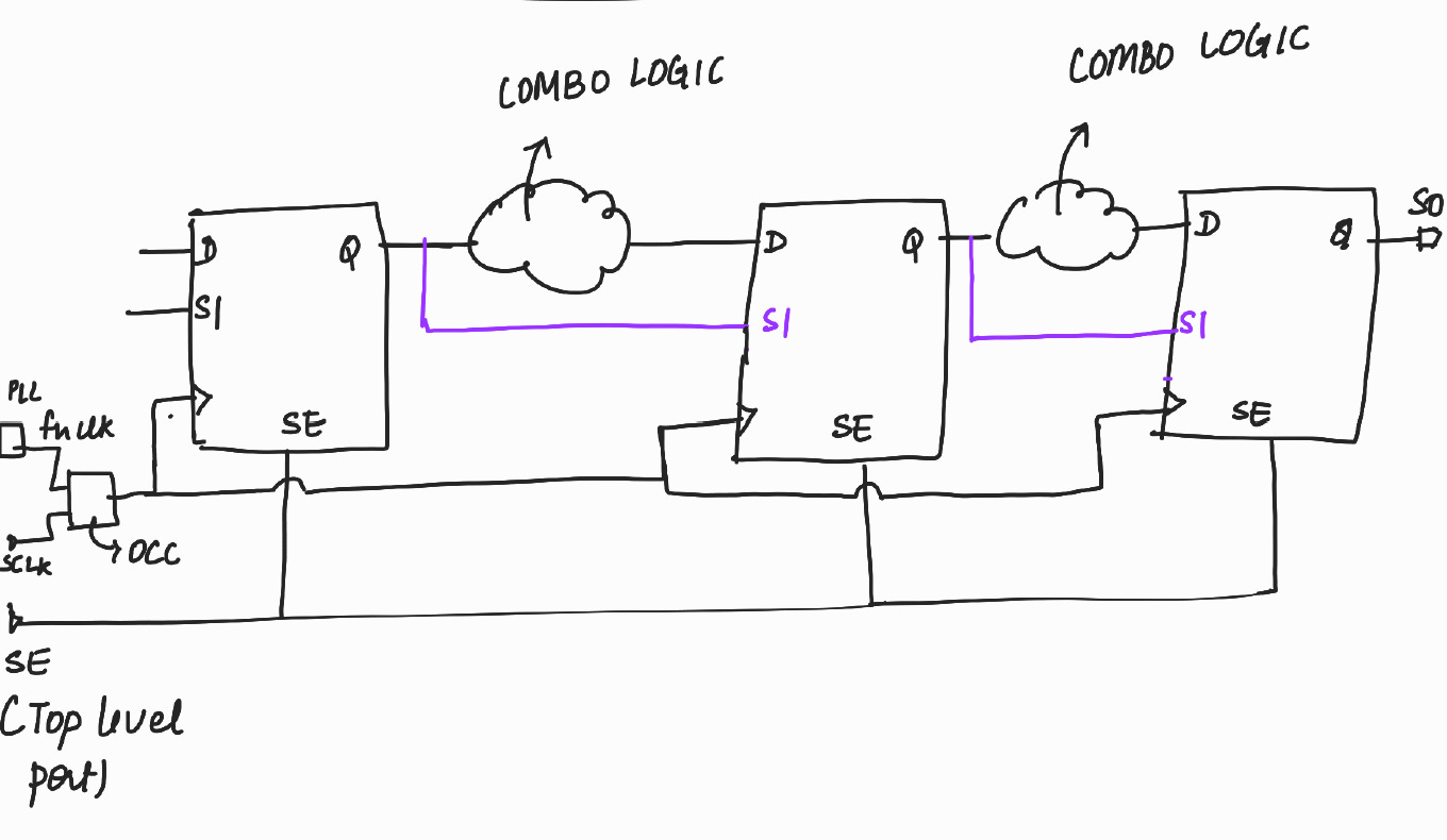
Scan Chain
Scan Chain Operation
Scan chain operation involves 3 stages :
Scan-in
Scan-capture
Scan-out
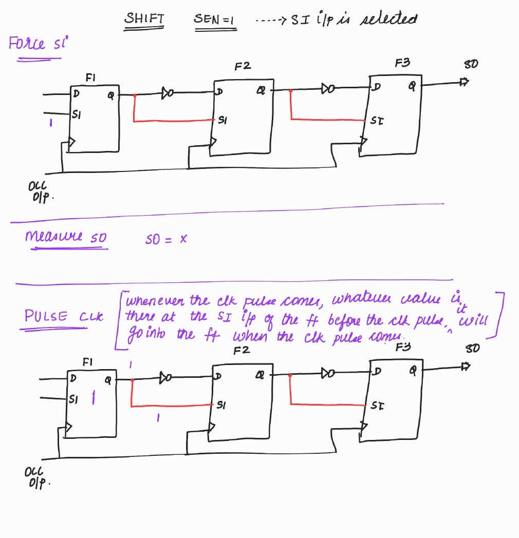
Scan-in involves shifting in and loading all the flops with an input vector. During scan-in, the data flows from the output of one flop to the scan-input of the next flop like a shift register.
Once the sequence is loaded, one clock pulse (also called as capture pulse) is allowed to excite the combinational logic block and the output is captured at the second flop. This is the Scan-capture phase.
The data is then shifted out and the signature is compared with the expected signature. This is called Scan-out phase.
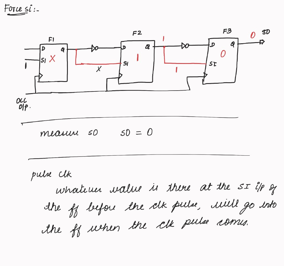
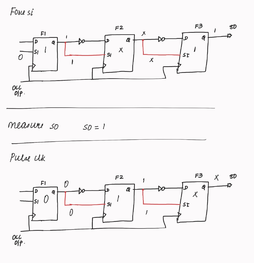
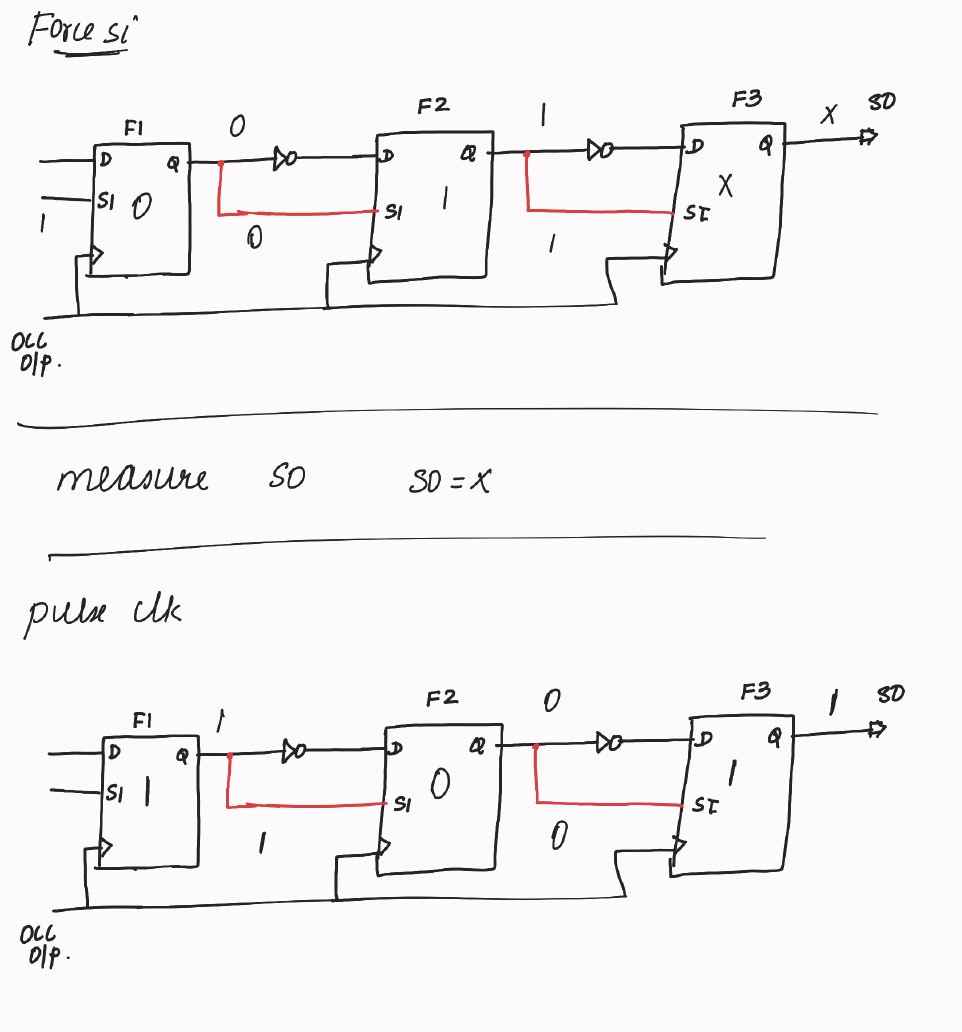
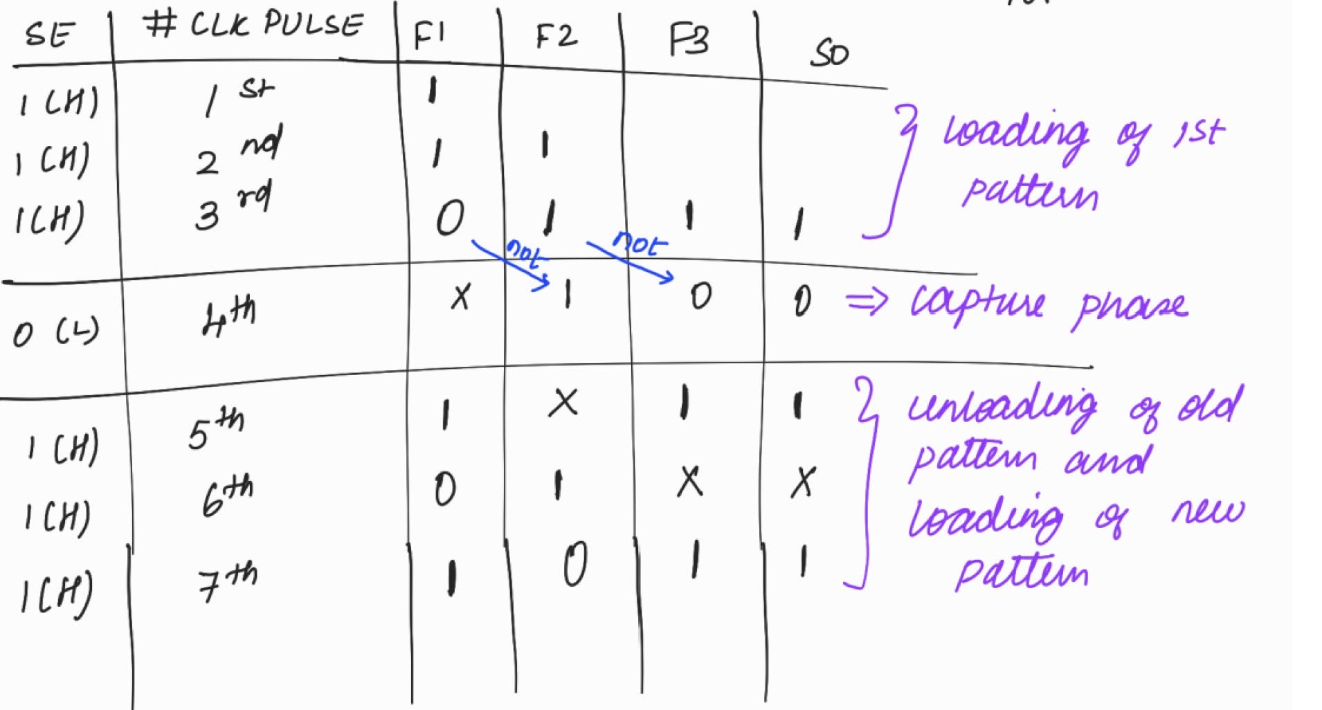
Let’s try to understand the scan chain operation with an example.
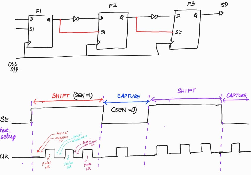
No. of clock pulses in the shift phase = No. of flops in the scan chain
No. of clock pulses in the capture phase = 1
Let’s assume 2 patterns for this illustration
P1 : 011
P2 : 101
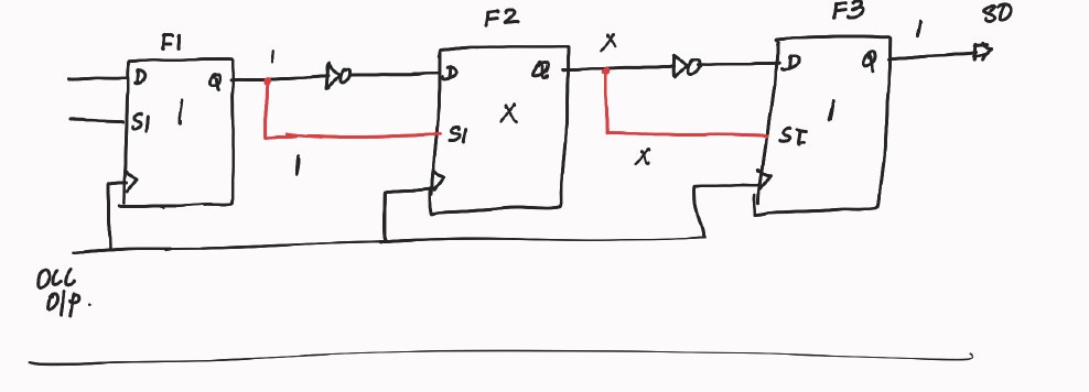
During the first shift phase, P1 will be loaded into the scan chain.
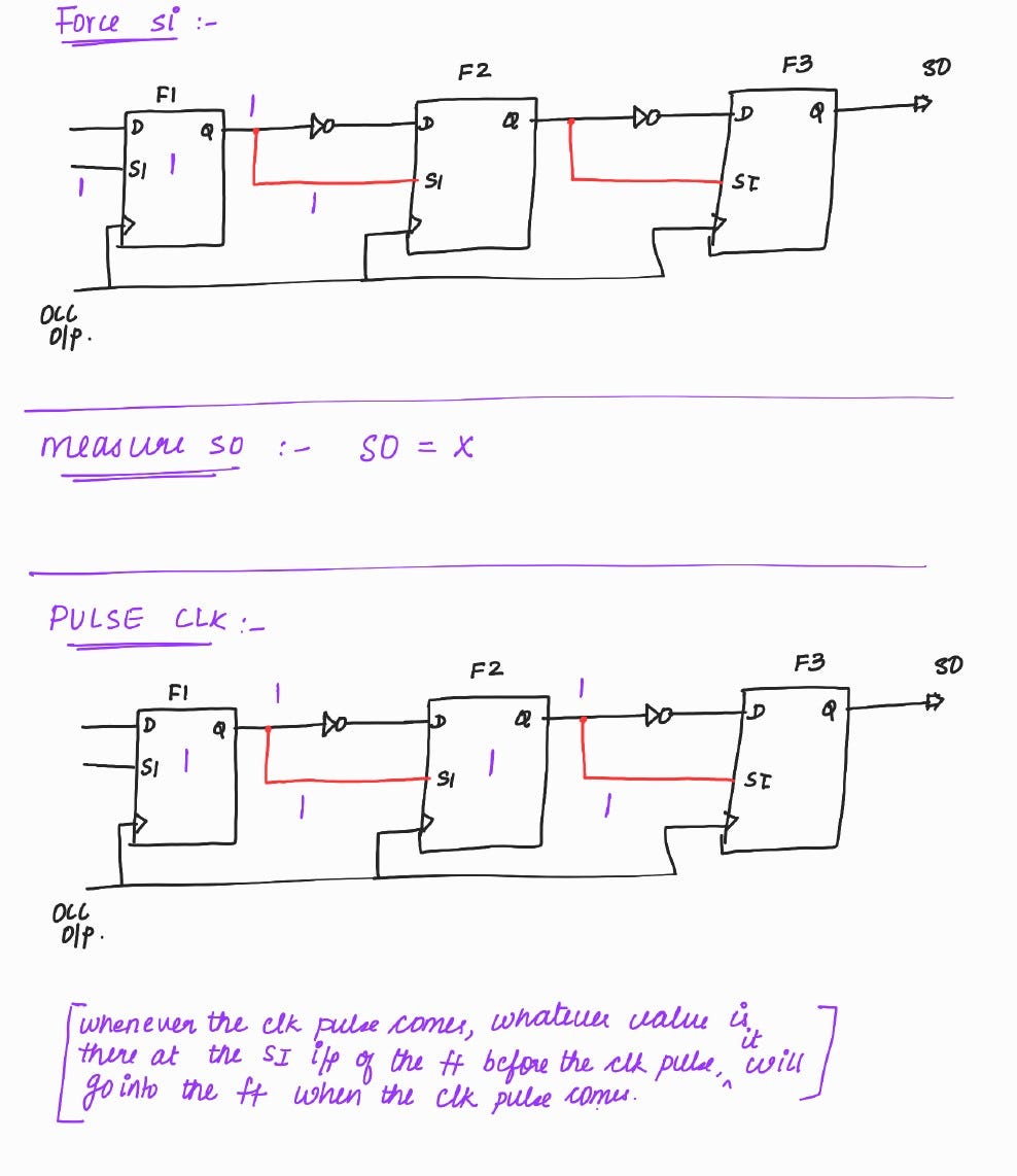
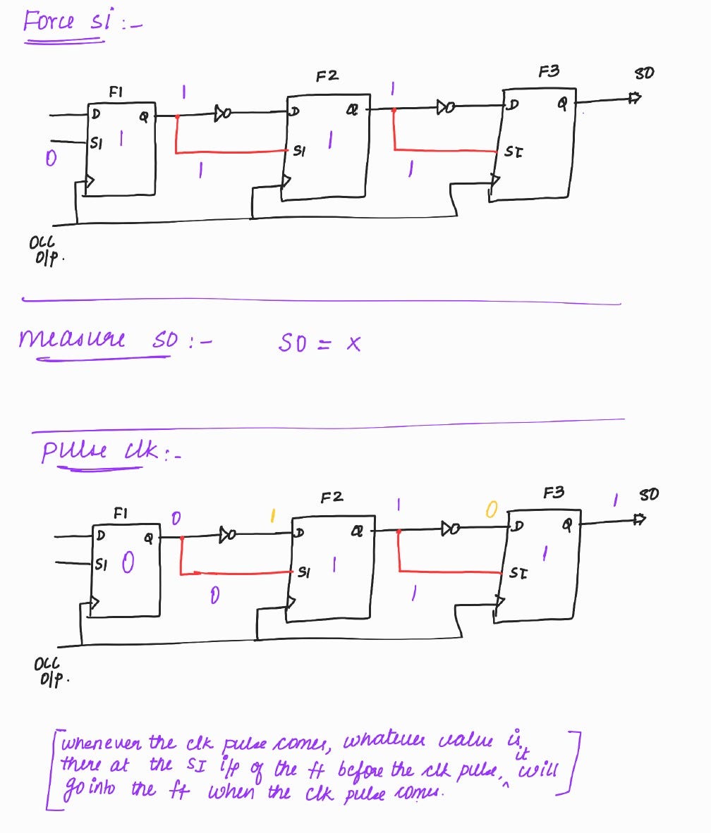
After 3 clock pulses in this example, we have loaded the first pattern into the scan chain.
Capture Phase :
The response of the combo logic will be captured into the flop.
i.e., the last shifted value of F1 through the combo logic will be captured by F2.
The last shifted value of F2 through the combo logic will be captured by F3.
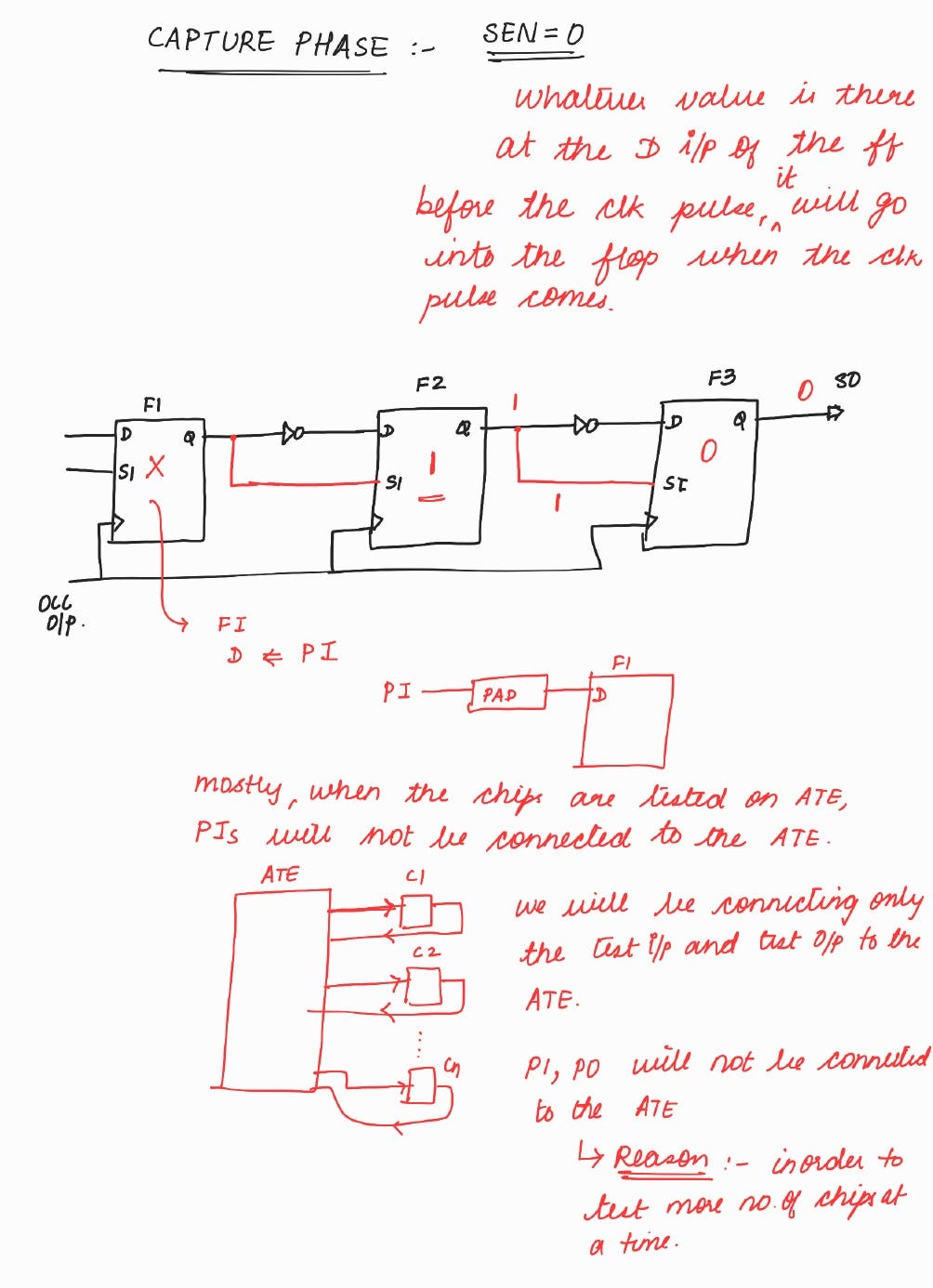
During the second shift phase, captured value of P1 will be shifted out and simultaneously P2 will be shifted into the scan chains.


Summary of Scan Chain Operation
Pattern 1 : 011
Pattern 2 : 101
Significance of the ‘measure so’ phase
During measure so phase, the value at the SO will be compared with the expected value (the ATPG tool while writing the patterns, will give the input sequence and expected output).
If suppose, there was some defect in the combo logic, then a wrong value would be captured and shifted out. The value measured at the SO will be different from the expected value.
Note :
During scan insertion : (Before manufacturing)
Normal flops will be converted to Scan flops and scan chains will be stitched.
During ATPG : (Before manufacturing)
Test patterns will be generated (consisting of the input sequence and expected output)These test patterns will be used to test the chip after manufacturing.
After manufacturing, chips will be tested on ATE (Automatic Test Equipment)Input sequence will be applied onto the chip.
Output of the chip will be compared with the expected output.If the Output of the chip == Expected Output, it means that the chip is good.
If the Output of the chip != Expected Output, it means that the chip is faulty. There are some manufacturing defects in the chip.
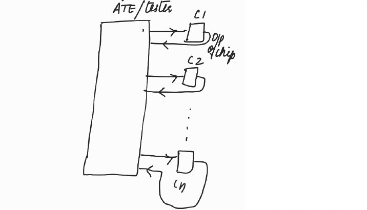
Illustration of the significance of the ‘measure so’ phase
According to the values taken in the above illustration, the expected value is written as
SO = XXX01X
Suppose during manufacturing, a defect has occurred as shown below :

Let’s assume 2 patterns for this illustration
P1 : 011
P2 : 101
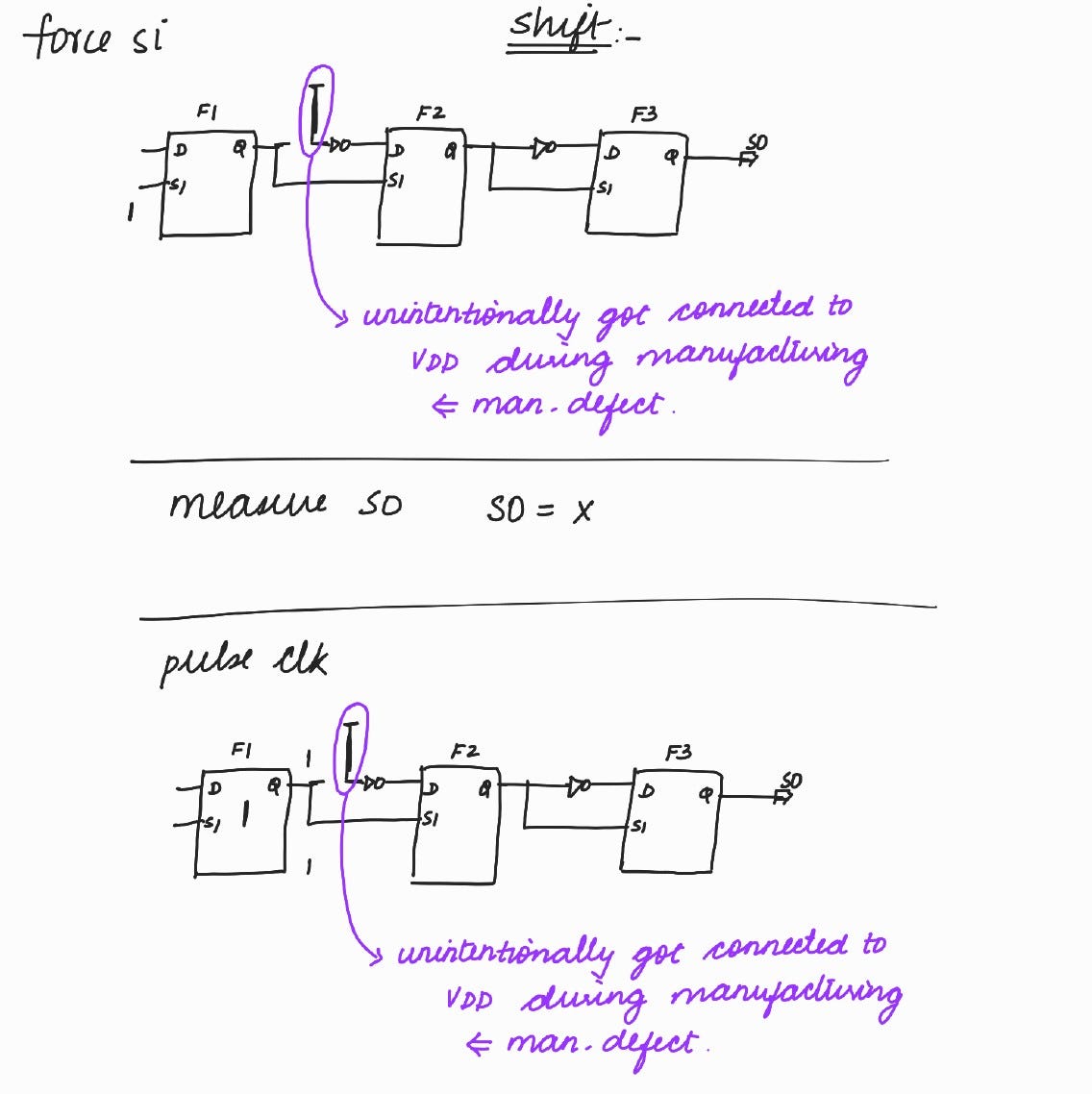


Wrong Value due to the manufacturing defect.
The chip has failed on the ATE. ATE will generate a failure log.
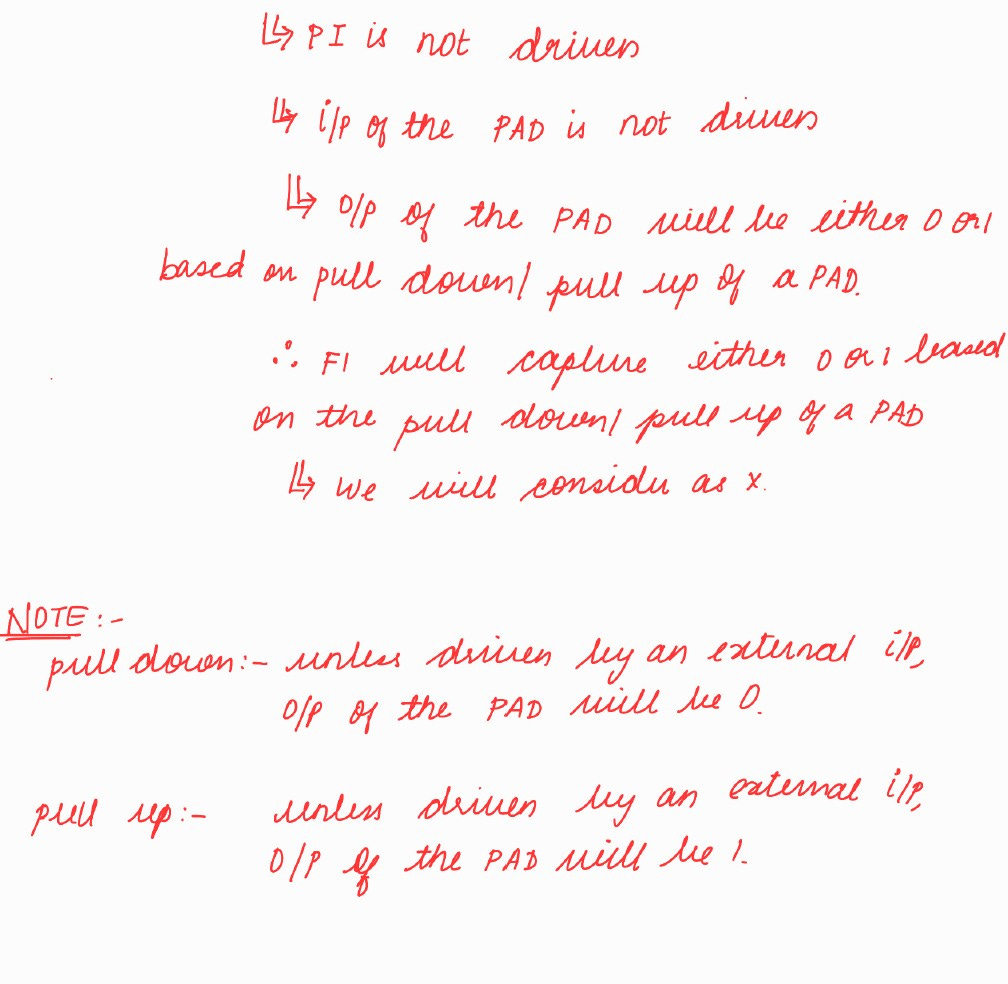
How do you find out exactly which combo the defect is in?
If we give the Verilog file, ATPG test patterns that were used on the tester and the failure log to the diagnostics tool, it will tell what manufacturing defect has caused the chip to fail.
How is the diagnostics tool able to give this info?
This is because the DFT team generates patterns using fault simulation.
< <We will explore fault simulation in ATPG topic > >
Scan insertion is a crucial step in the DFT flow. It enables the conversion of flops into scan flops and incorporates scan flops in scan chains.
We have explored how scan chains operate to facilitate efficient testing.
However, why is scan insertion necessary in the first place? What challenges does it address, and how does it improve testability?
very much thanku for this blog
Thanks @vidisha for share your knowledge...! it helped me to understand better..!