In my recent blogs, I’ve been covering various aspects of EDT (Embedded Deterministic Test) logic—exploring components like the decompressor, compressor and controller logic. While there are still a few important EDT topics left to discuss, I’ll be taking a brief detour in this post to focus on another critical element of DFT infrastructure: the On-Chip Clock Controller (OCC).
Let’s get started!
On-chip clock Controller (OCC) :
On-Chip Clock Controller (OCC) is a circuit that decides
the clock to be propagated during functional mode and the clock to be propagated during DFT mode (during shift phase and during capture phase)
the no. of clock pulses to be propagated during capture phase.
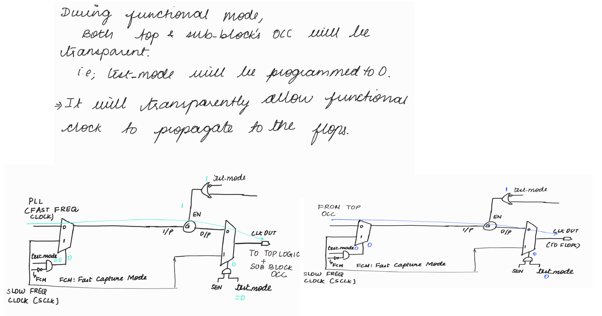
In Functional mode, Functional clock will be propagated.
In DFT mode, In Shift phase → SCLK (Low frequency clock) In Capture phase,
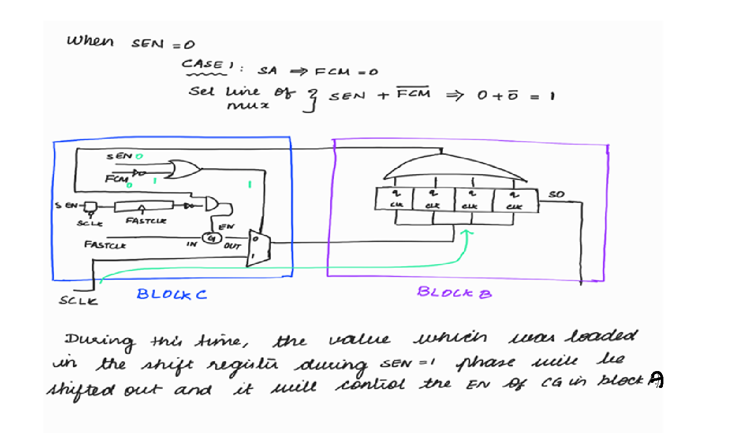
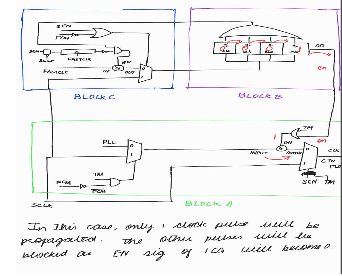
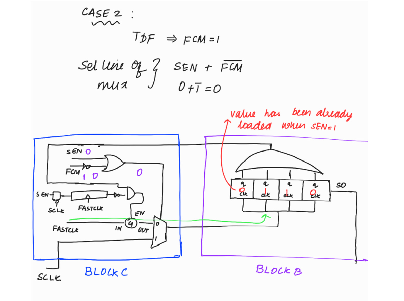
SA Fault Model → SCLK (1 clock pulse) Transition Delay Fault Model → Functional clock (2 clock pulses)
<< We will explore about Fault models during ATPG topic. >>
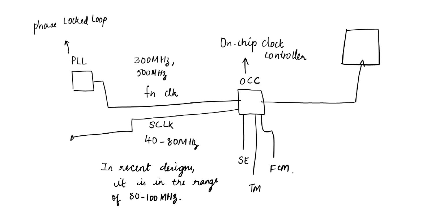
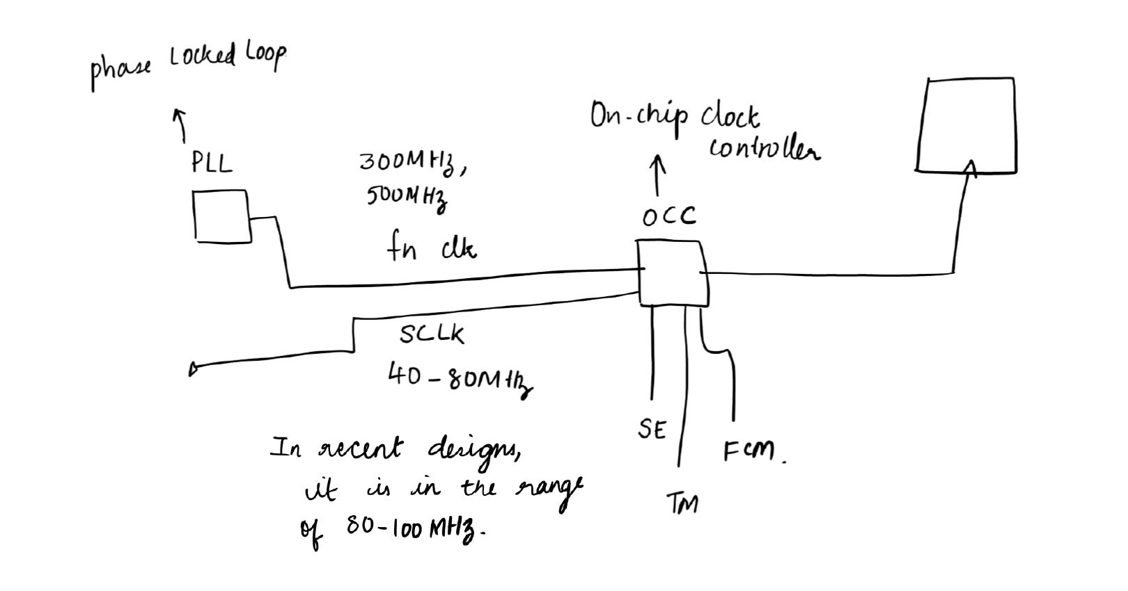
where, fn clk stands for Functional clock. It will be a high frequency clock (Example, 300 MHz, 500 MHz) and SCLK stands for Scan clock. It will be a low frequency clock (usually around 40-80 MHz . In the recent designs, it is in the range of 80-100 MHz).
OCC decides whether Functional clock (fn clk) or Scan Clock (SCLK) has to be propagated to the flops, based on the values of SE (Scan Enable), TM (Test Mode), FCM (Fast Capture Mode) signals.
Let’s explore the structure of Tessent OCC !
Note :
The OCC structure explained in this blog is a simplified representation of Tessent OCC designed to help freshers understand the concept easily. It does not reflect the exact internal implementation used in Tessent OCC.
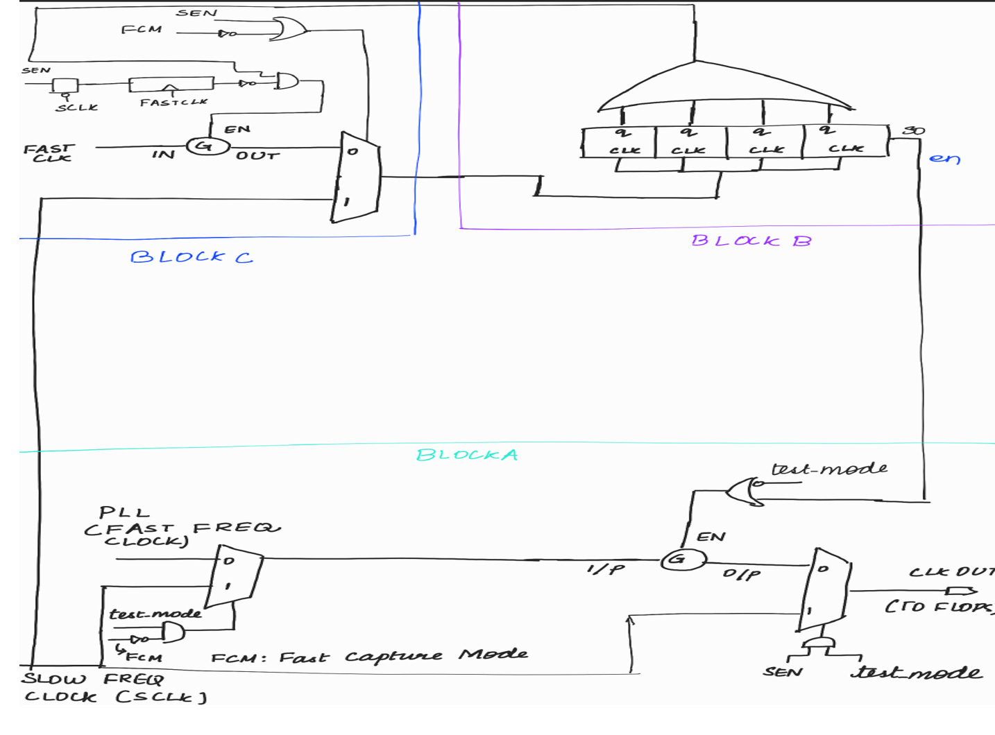
I have divided the OCC architecture into 3 blocks:
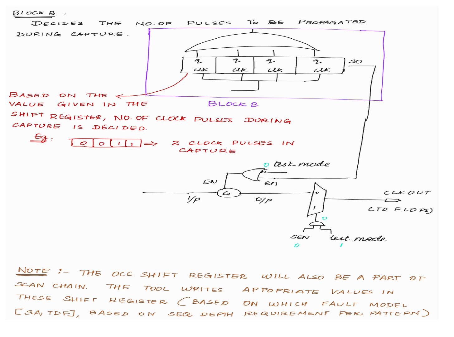
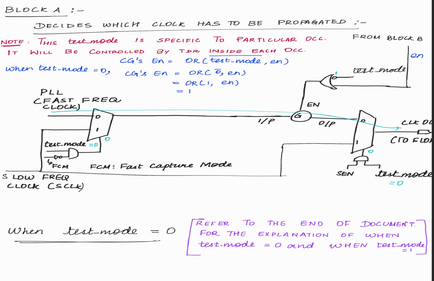
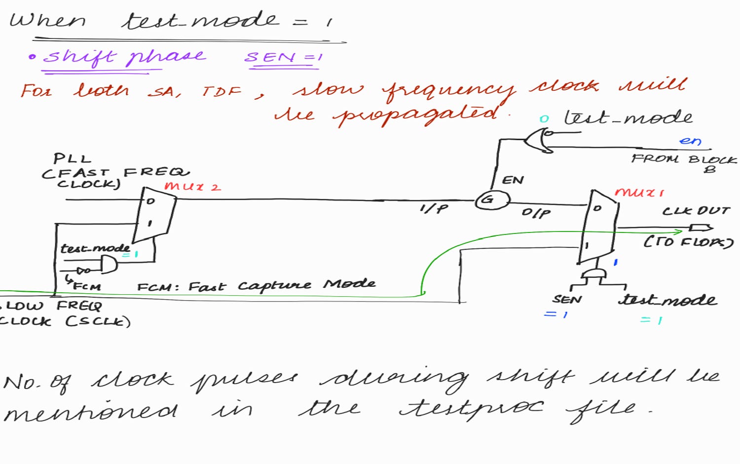
BLOCK A : Decides which clock has to be propagated to the flops. BLOCK B (OCC shift register flops) : Decides the no. of clock pulses to be propagated during capture phase.
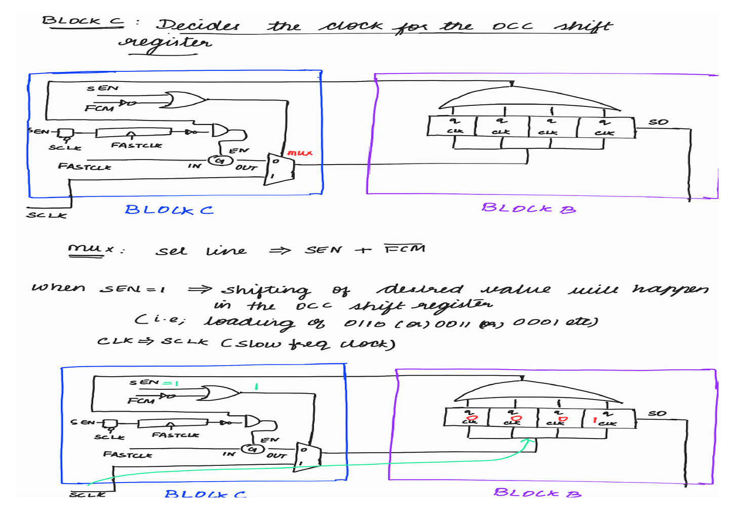
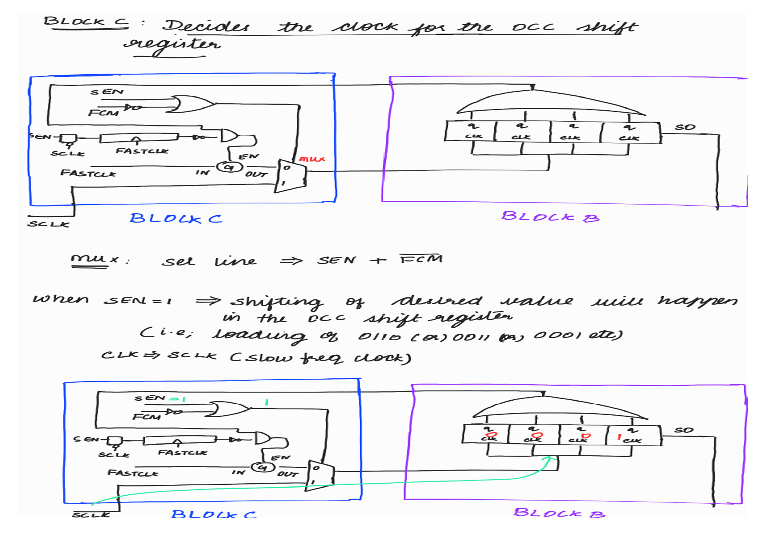
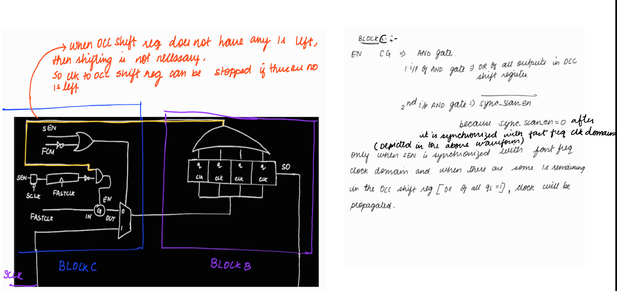
BLOCK C : Decides the clock to the OCC shift register flops.
Let’s explore each block in detail !
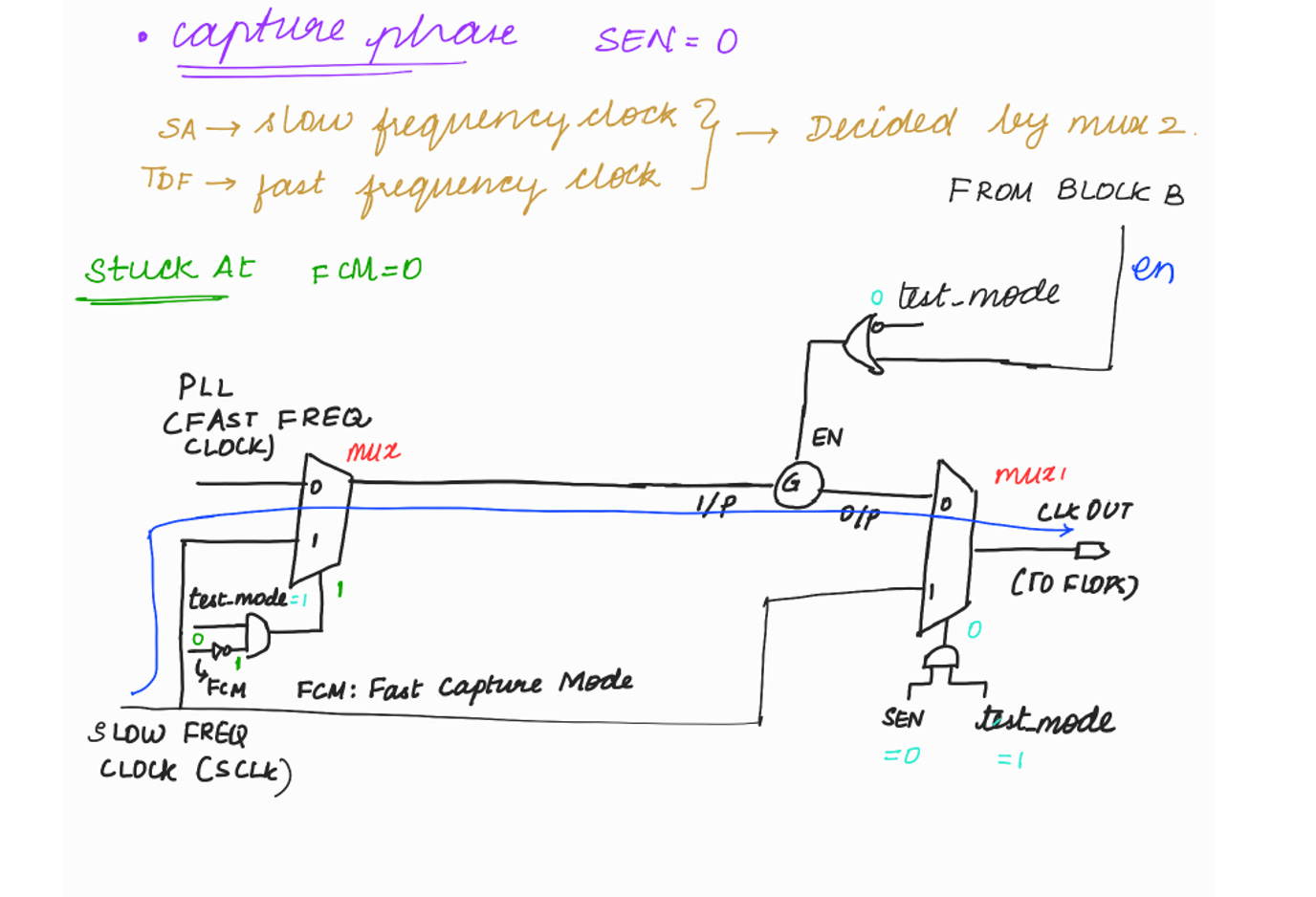
BLOCK A:
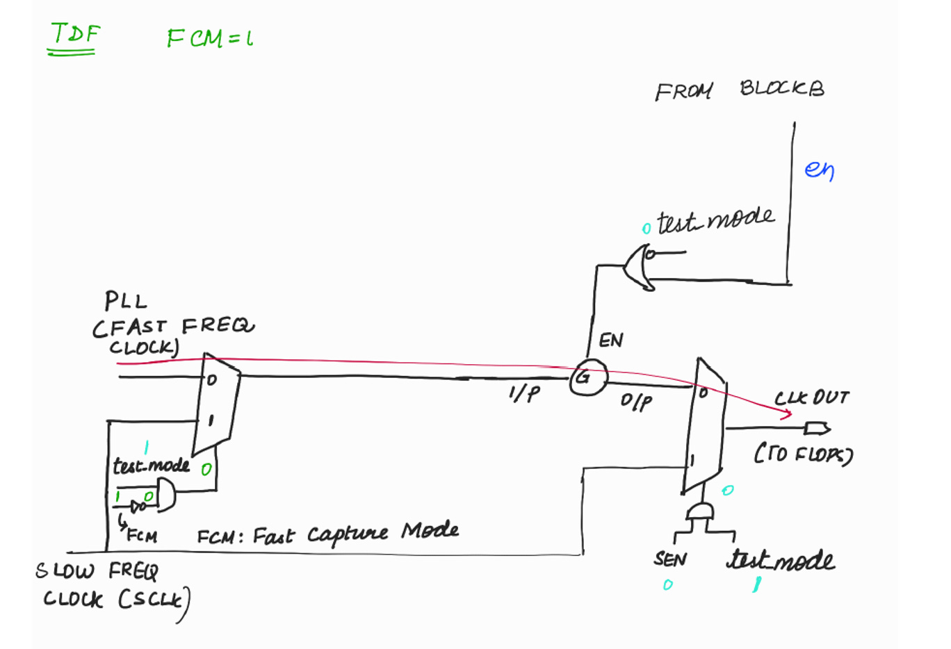
where, SA stands for Stuck-at Fault model and TDF stands for Transition Delay Fault model. < < We will explore about fault models in detail during ATPG topic. > >
As demonstrated above, during shift phase, both for Stuck at fault model and Transition Delay fault model, low frequency clock (or Slow frequency clock) (SCLK) will be propagated to the flops. We have explored the reason of why low frequency clock (or Slow frequency clock) has to be propagated during the shift phase in DFT Basics : Article #4
As demonstrated above, during capture phase, low frequency clock (or Slow frequency clock) is propagated to the flops for Stuck at fault model. < < We will explore the reason during ATPG topic > >
As demonstrated above, during capture phase, fast frequency (or high frequency clock) is propagated to the flops for Transition Delay fault model. < < We will explore the reason during ATPG topic > >
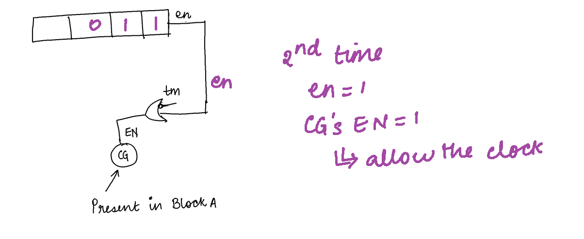
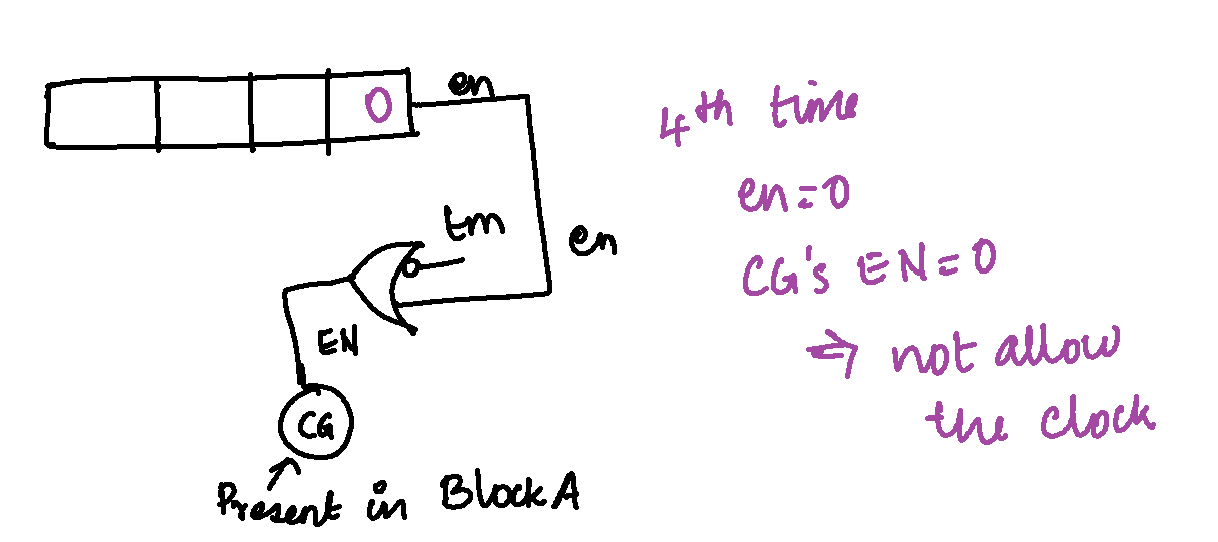
BLOCK B: OCC Shift Register flops
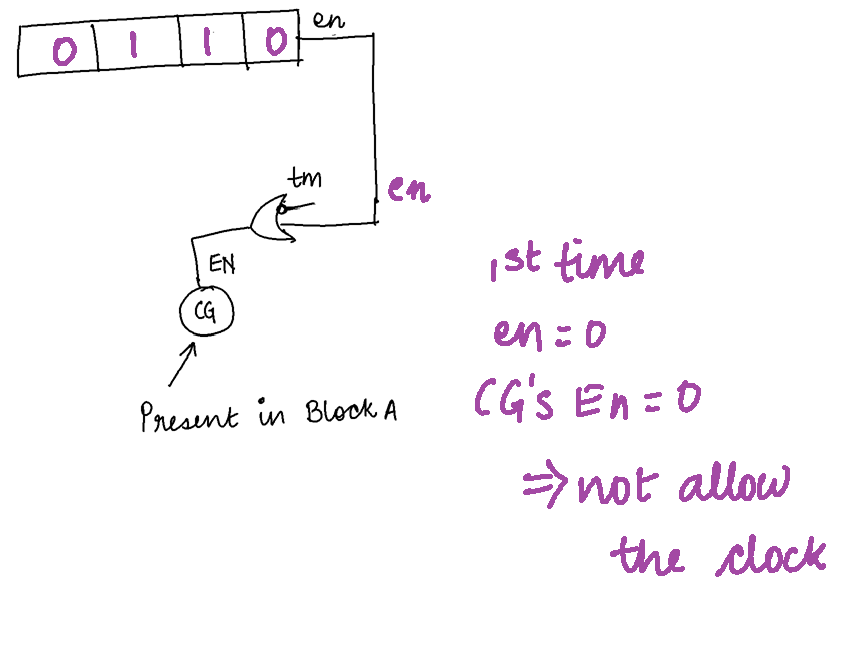
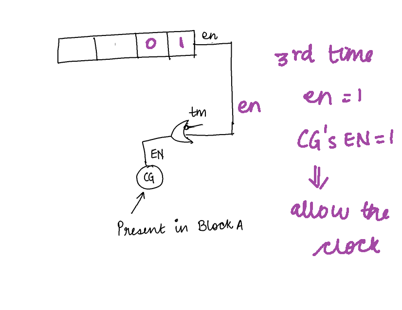
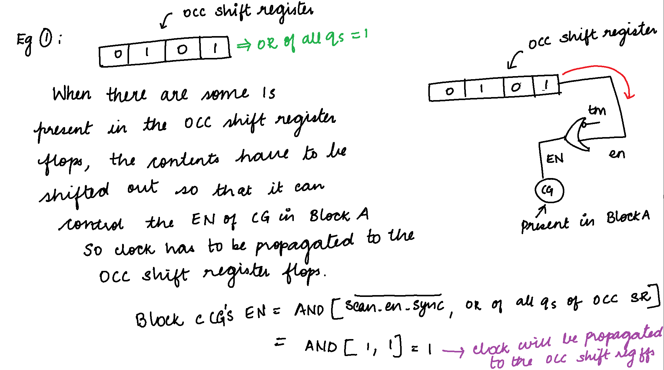
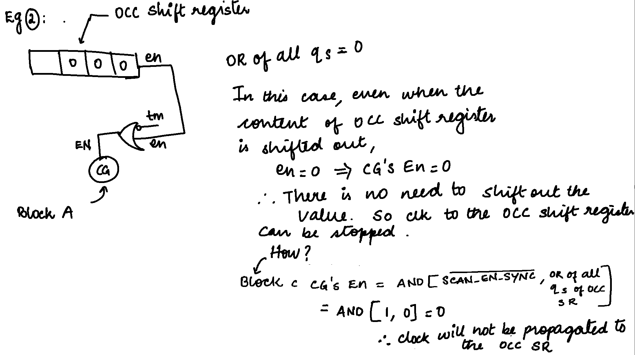
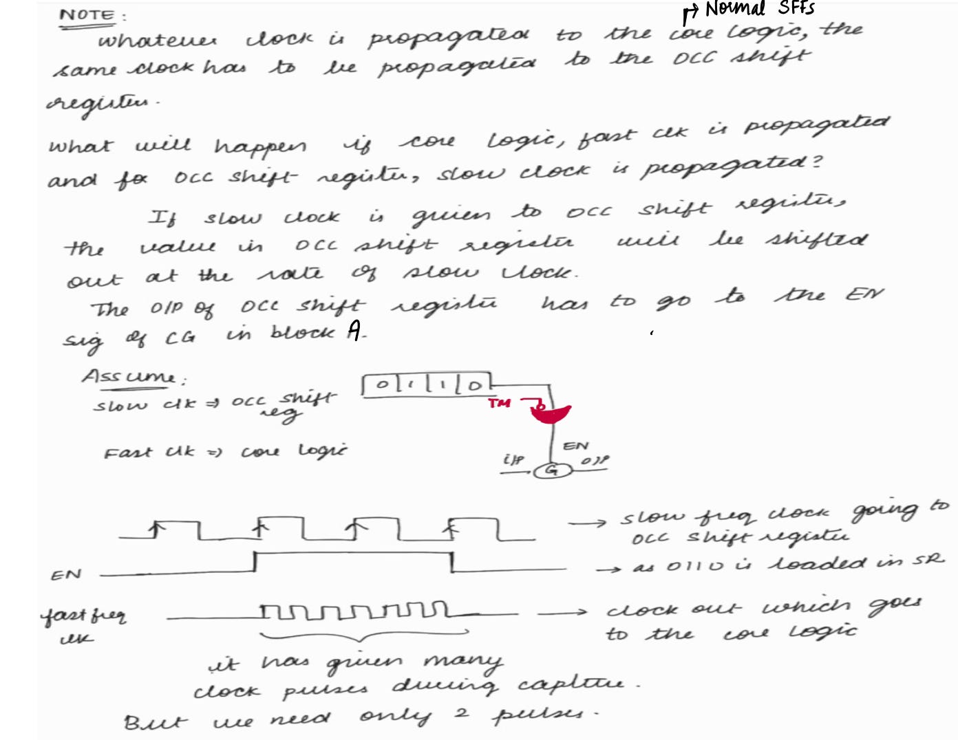
Based on the no. of 1s present in the OCC shift register flops, that many no. of clock pulses will be propagated during the capture phase.
Let’s try to explore it using the below illustration.
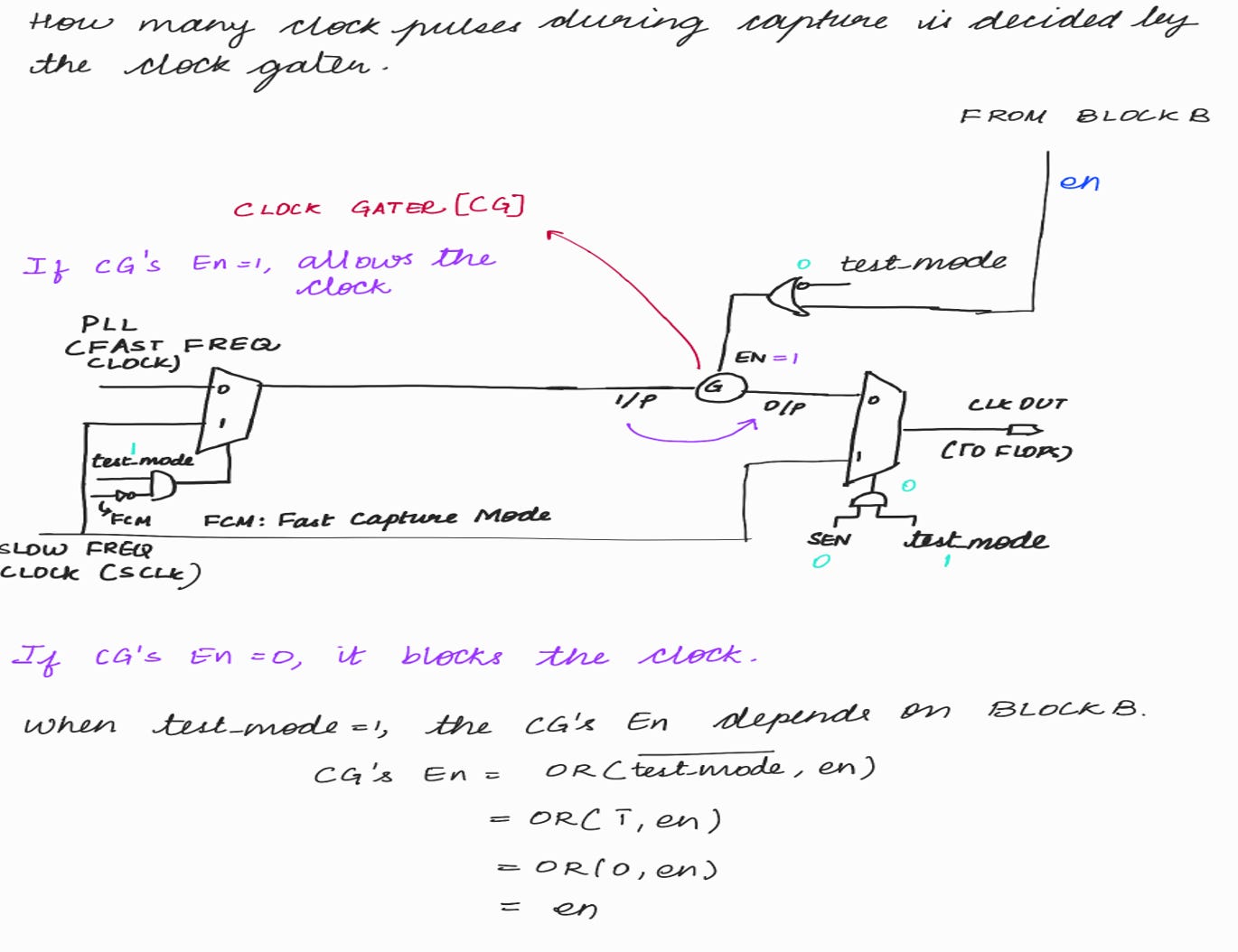
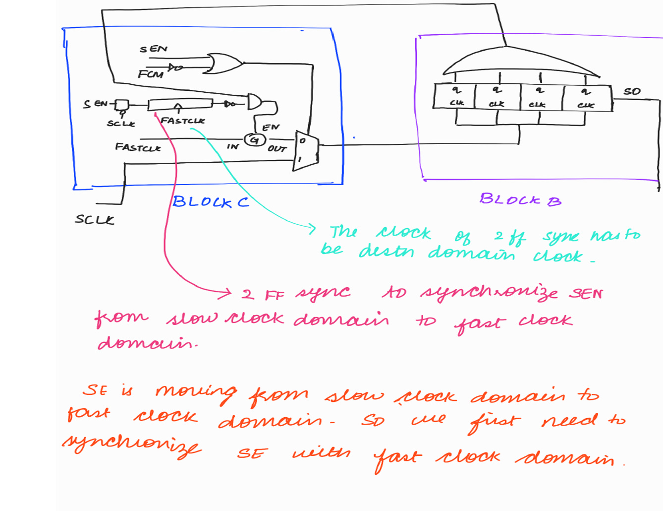
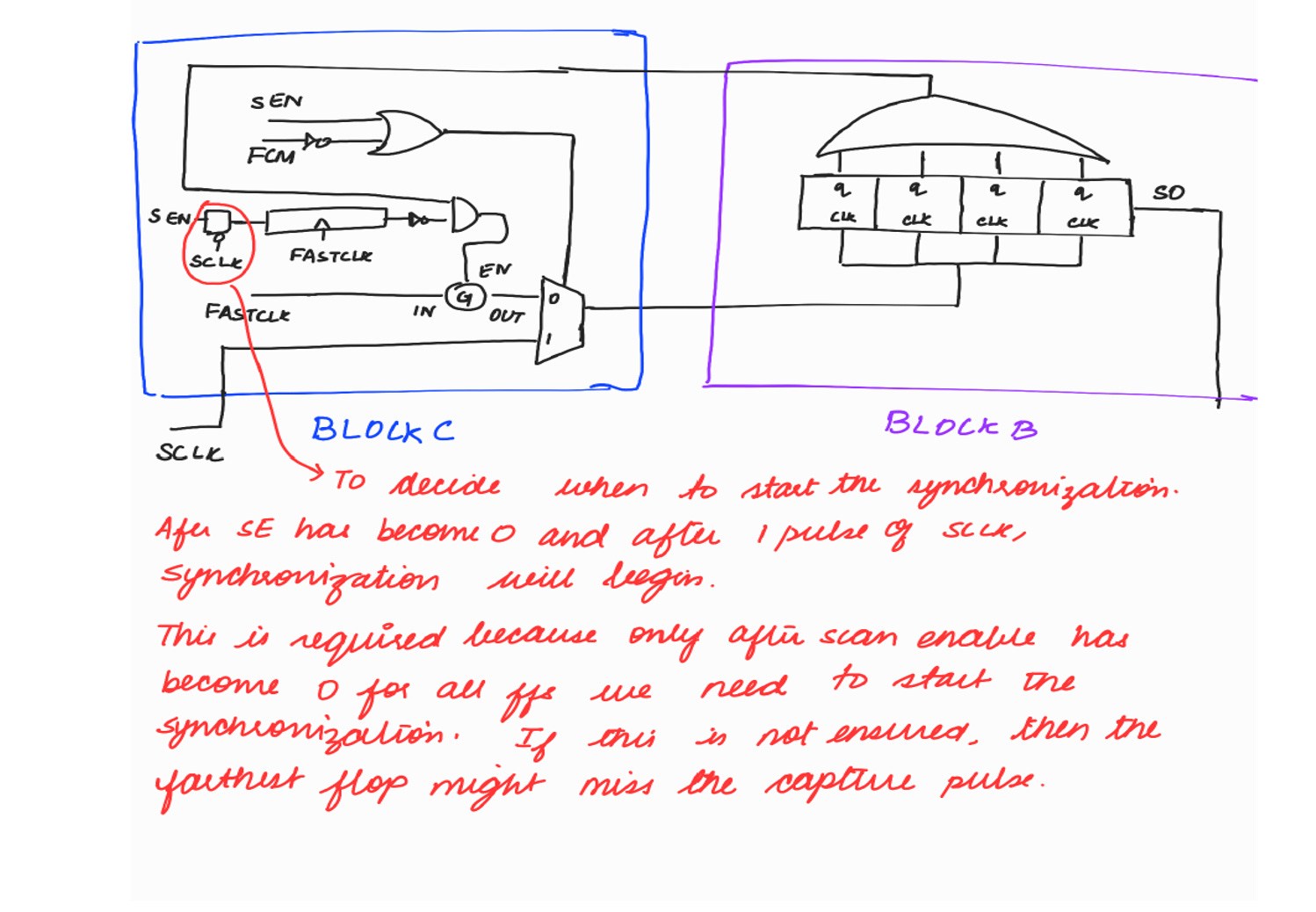
BLOCK C:
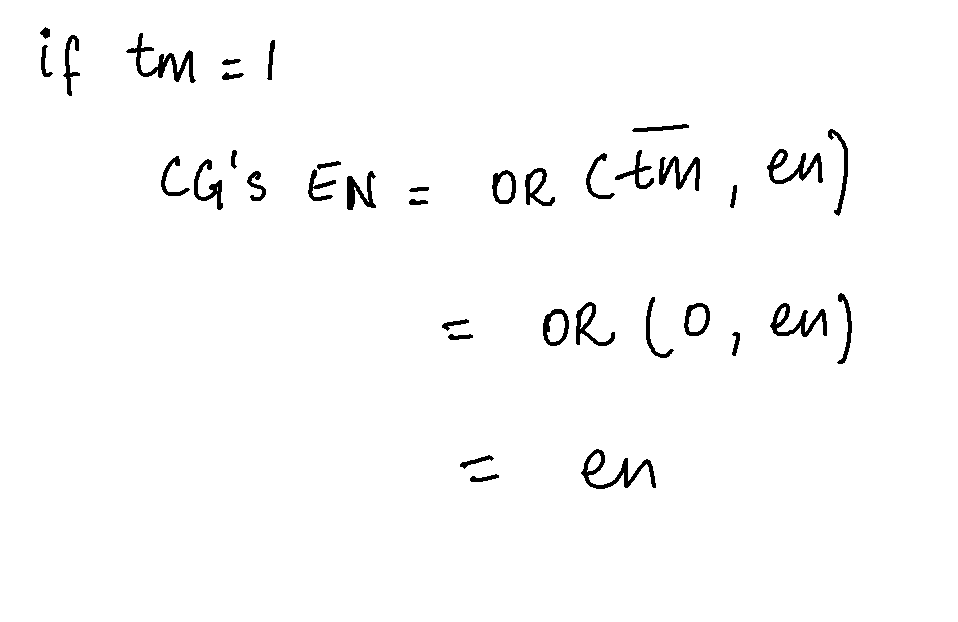
Let’s explore the Clock Gater (CG) which is present in the above path.
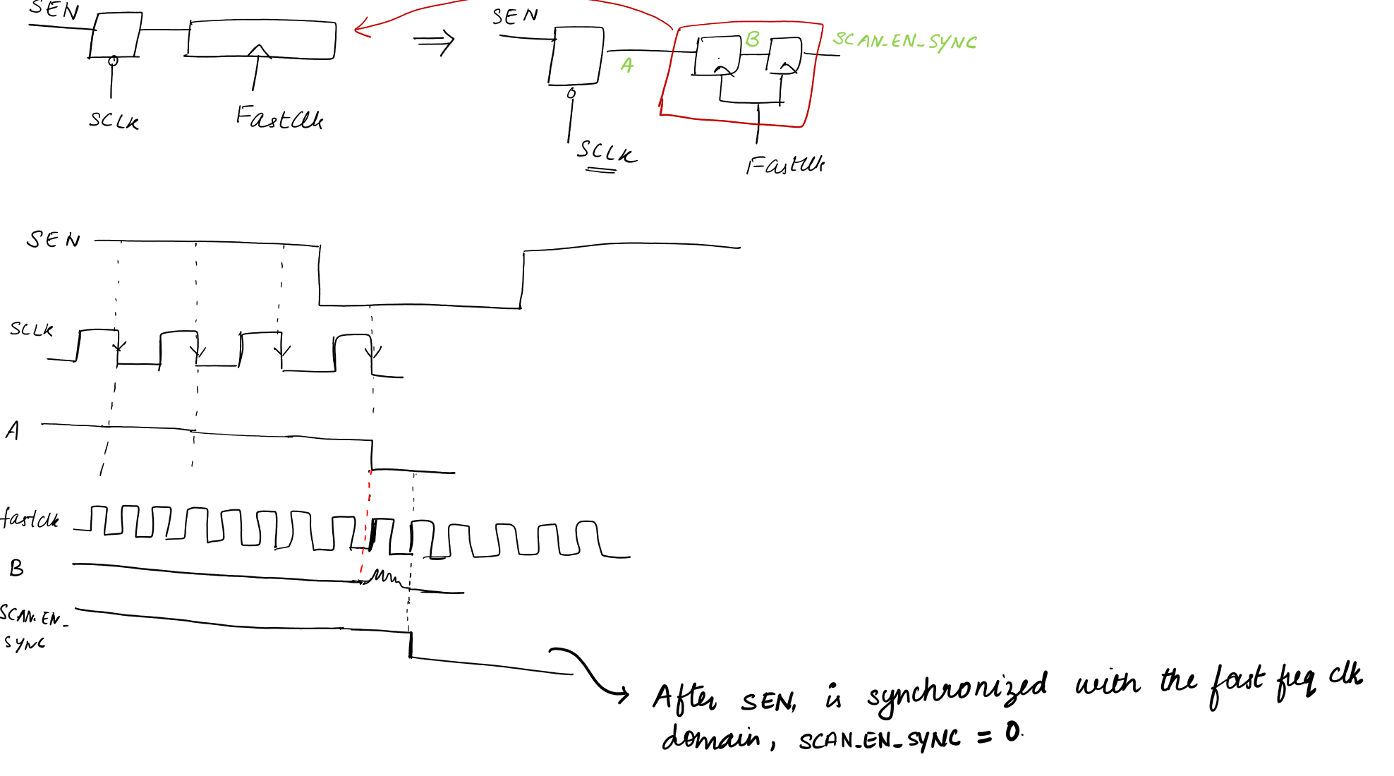
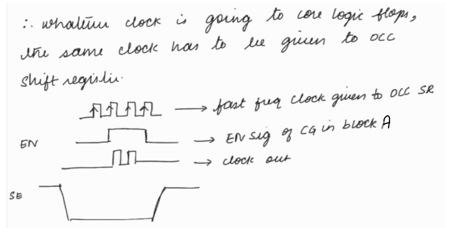
Why do we need to synchronize the SEN (Scan Enable) in OCC?
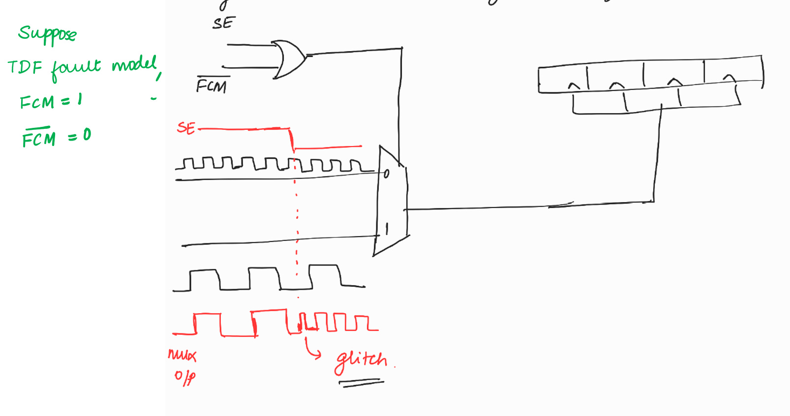
If we don’t synchronize the SEN in OCC, it will produce glitches as explained below:
Note 1 :
Note 2 :
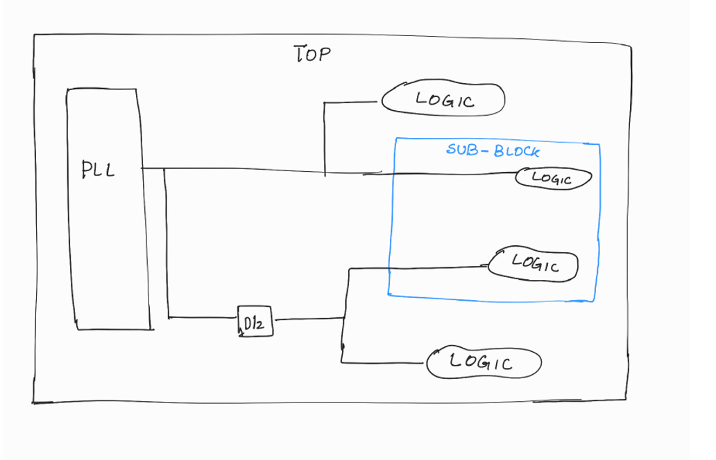
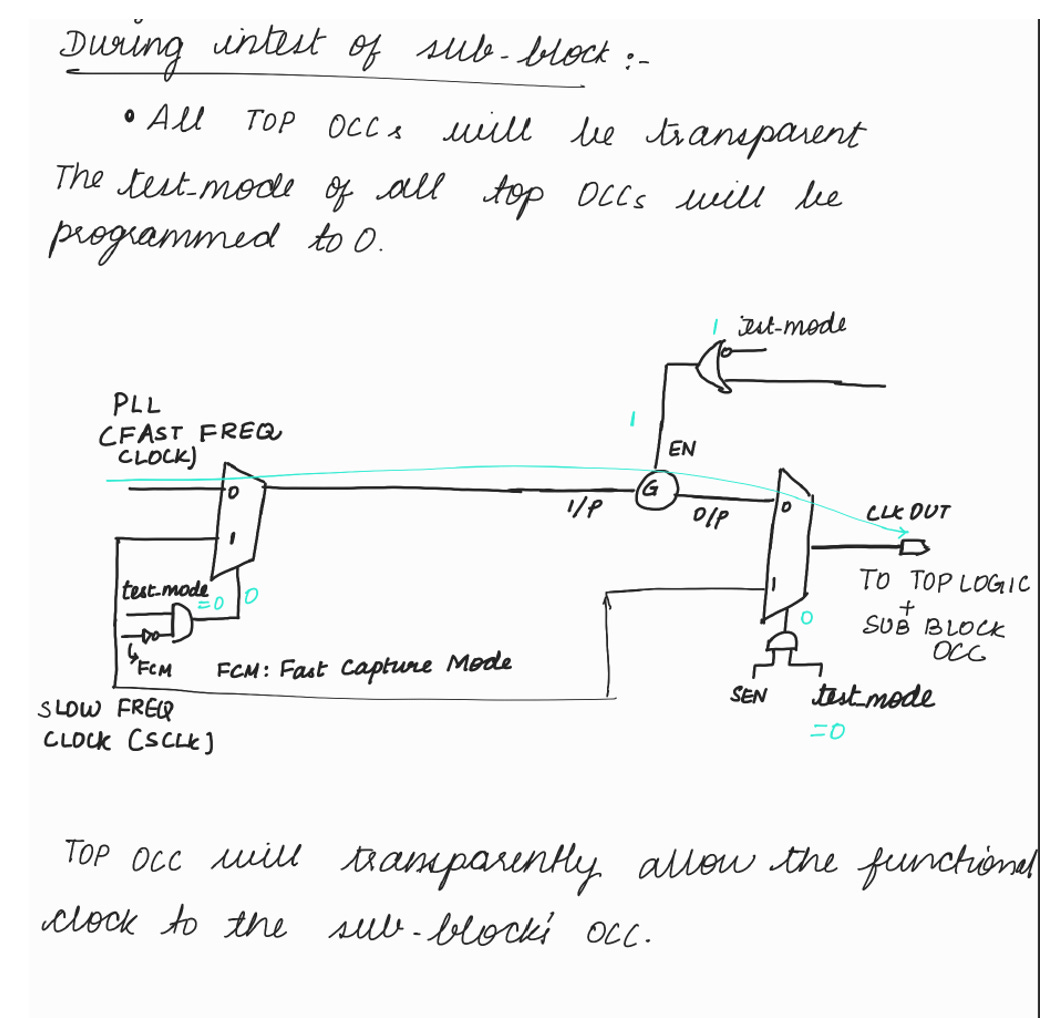
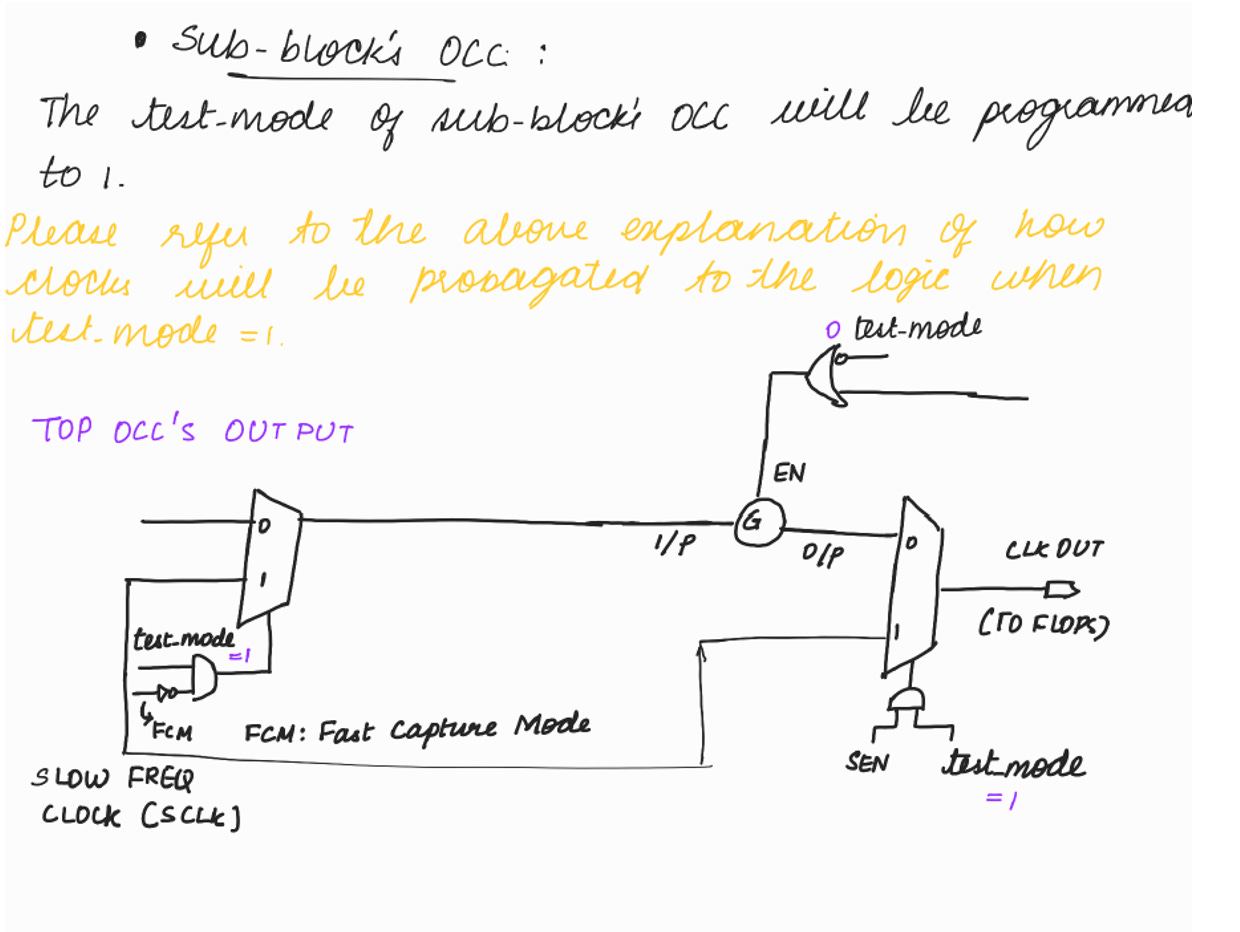
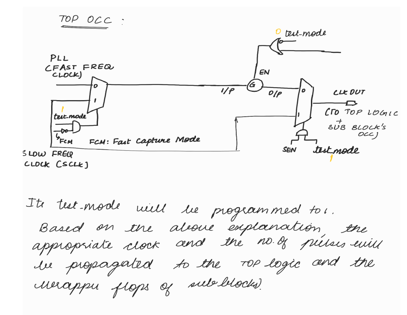
PLACEMENT OF OCC :
Let’s try to explore on the placement of OCC using the below example:
DESIGN :
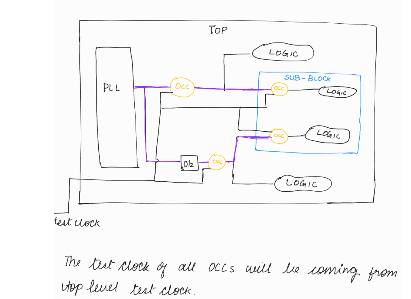
The output of PLL goes as the clock to some logics in the top and some logics in the sub-block. The output of PLL, through a frequency divide by 2 (D/2) logic, goes as the clock to some logics in the top and some logics in the sub-block. DESIGN AFTER PLACEMENT OF OCC:
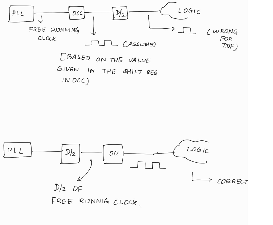
Note : Why do we need to place the OCC after the D/2 logic?
< < In this example, we will explore how clocks are propagated to the flops through the OCC during various modes. This explanation will eventually involve terms like INTEST and EXTEST.
However, for now, we will keep the focus on clock propagation itself. A more detailed discussion on INTEST and EXTEST will be taken up in a separate blog when we dive into the topic of Hierarchical Scan> >
In this blog, we had explored about the internal architecture of On-chip Clock controller (OCC) logic. We have explored how appropriate clocks and appropriate no. of clock pulses are propagated during various modes.
In my next blog, we will continue our discussion on EDT logic.
Stay Tuned - the next blog will be published this coming Sunday!
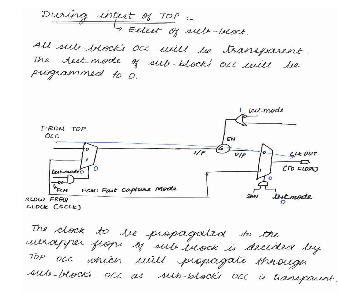
Yes. In hierachical scan, the OCCs will be placed in that way.
In the case which you are asking (it will be intest of TOP and extest of sub-block case), there sub-block's OCC will be transparent (tm = 0). So whatever clock is propagated by TOP OCC will transparently pass through sub-block OCC and go to the wrapper flops of sub-block as sub-blocks' OCC is transparent.
For diagrammatic explanation, you can check in the intest of TOP and extest of sub-block topic in placement of OCC topic.


I will discuss that in the ATPG topic.
I will discuss that when I cover the advantages of connecting TE of ICG to Scan Enable signal
Hi Shri,
Yes. In hierachical scan, the OCCs will be placed in that way.
In the case which you are asking (it will be intest of TOP and extest of sub-block case), there sub-block's OCC will be transparent (tm = 0). So whatever clock is propagated by TOP OCC will transparently pass through sub-block OCC and go to the wrapper flops of sub-block as sub-blocks' OCC is transparent.
For diagrammatic explanation, you can check in the intest of TOP and extest of sub-block topic in placement of OCC topic.