DFT Interview : Article #4


Welcome to the fourth post in this series !
You can also explore DFT Interview : Article #3
In DFT Basics : Article #5 and DFT Basics : Article #6, we have explored the various DRCs which we will encounter during Scan insertion.
In this post, we will explore some of the DRCs which we will encounter during ATPG.
Q: What are the DRC violations which you have encountered during ATPG?
Ans : Some of the DRC violations which we encounter during ATPG are Tracing violations (T rules), D1 violation
1. Tracing Violations :
Some of the tracing violations which we encounter during ATPG are T3, T5, T24 violations (while working with Tessent tools).
T3 violation : The shift procedure must create a sensitizable path from the scan chain output back to the scan chain input. An improperly sensitized gate in the scan path causes an error condition, which the tool reports as a T3 DRC violation.
T5 violation : During the shift procedure, you must never place an X value on a clock input or an active (X or 1) value on a set or reset input of a memory element in the scan path.
Now let’s explore some practical scenarios which can result in T3 and T5 violations :
Scenario 1:
< < In companies, there will be multiple intermediate releases before the final release > >
Suppose,
During first release :
Designer has used a set of flops.
Library file 1 contains the flop models used by the designer.
Library file 1 is read during Scan and ATPG.
During second release :
Designer has additionally added few more new flop models.
Library file 2 contains the additional new flop models used by the designer.
Both library file 1 and library file 2 is read during Scan.
During ATPG execution, the old setup was mistakenly used. In this setup (from the first release), only Library File 1 was read. As a result, the newly added flop models were treated as black boxes during ATPG.
In this situation, we will encounter T3 violation.
Solution : Read both the libraries (library file 1 and 2) during ATPG
Scenario 2:
Suppose, during the final release, the designer has manually added a new ICG (Integrated Clock Gating Cell) to reduce the dynamic power (he has done it after scan insertion without informing DFT). In addition, the Test Enable (TE) pin of the ICG was not properly controlled.
In this scenario, we will encounter T3 and T5 violations
Solution :
Connect the TE of ICG to Test Mode [TM] (or)
Connect the TE of TCG to Scan Enable (SE) → This is advantageous
To explore more on ICG, please check DFT Basics : Article #4
To explore more on the fix, please check Answering Curious Minds
Now let’s explore some practical scenarios which can result in T24 violation:
If we have not added a lock up latch for domain mixing, it will result in T24 violation.
To explore more on domain mixing and why a lock up latch is needed during domain mixing, please check DFT Basics : Article #9
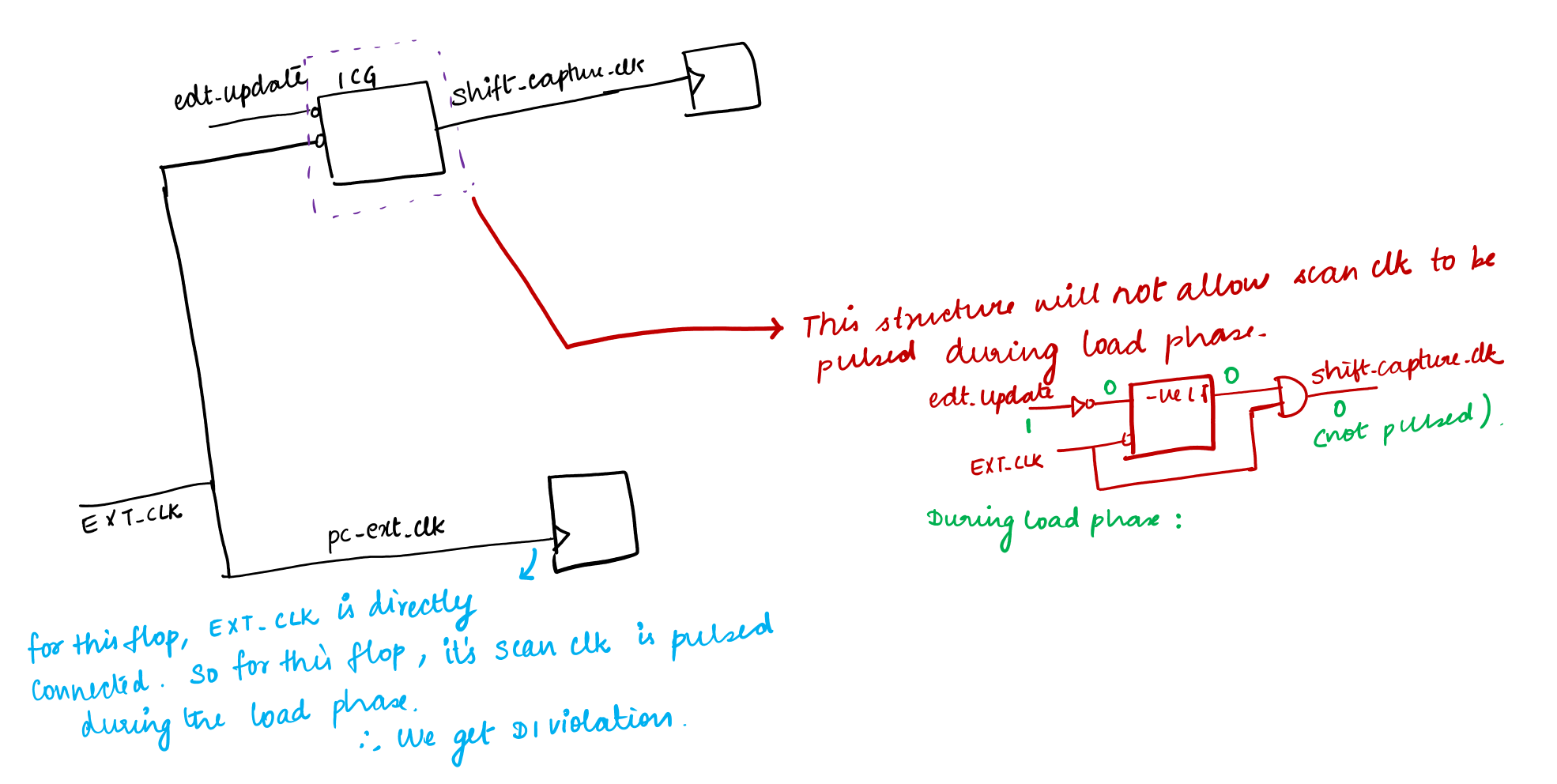
D1 violation :
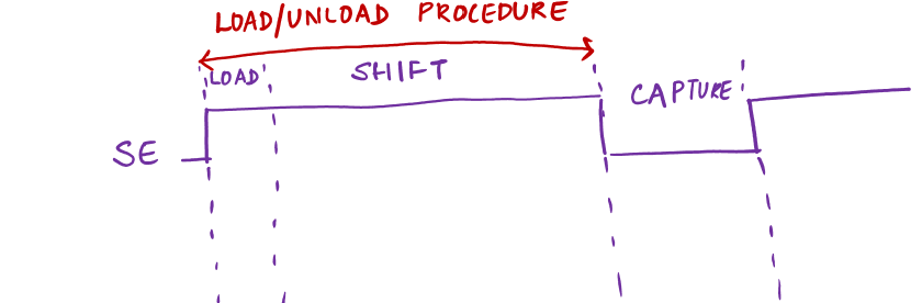
If a Scan clock is pulsed during the load phase, it will result in D1 violation.
< < Note: In load phase, only edt_clock and edt_update has to be pulsed > >To explore the reason of why scan clock should not be pulsed during load phase, please check DFT interview : Article #1 (Question 3)
To explore more on EDT logic, please check my DFT Basics Article 11 to 17.
Now let’s explore some practical scenarios which can result in D1 violation:
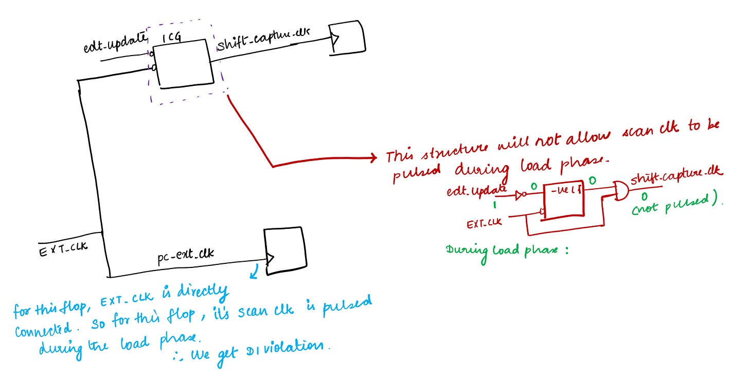
< < To understand the ICG structure used in the above figure using a waveform, please check DFT Interview : Article #3 (Question 9 ) > >
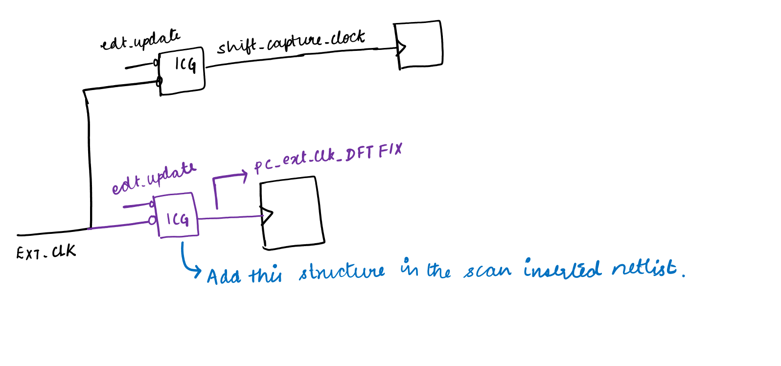
Solution :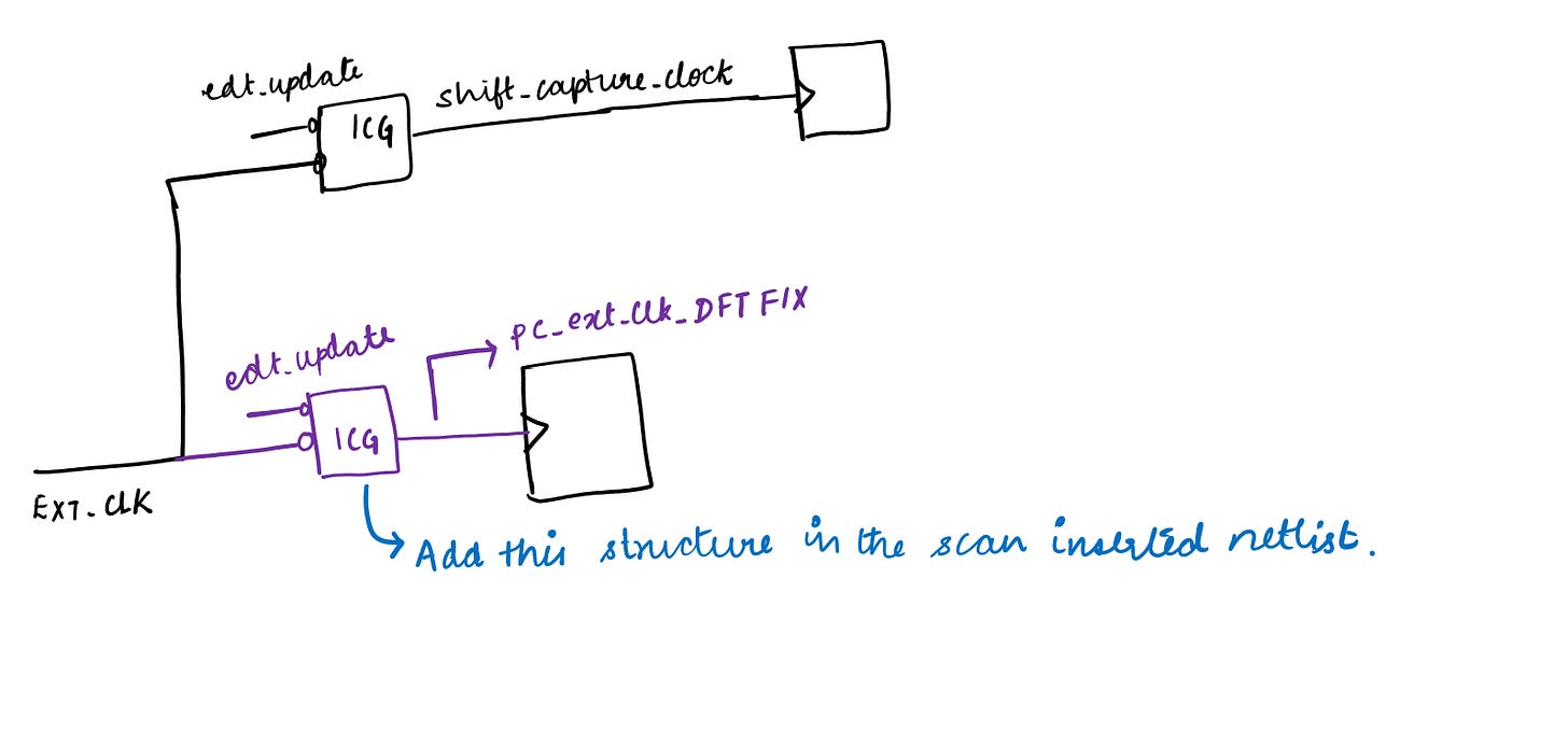
References :
Tessent Scan and ATPG user’s manual